SLVSDR9E October 2016 – January 2021 DRV8702-Q1 , DRV8703-Q1
PRODUCTION DATA
- 1 Features
- 2 Applications
- 3 Description
- 4 Revision History
- 5 Pin Configuration and Functions
- 6 Specifications
-
7 Detailed Description
- 7.1 Overview
- 7.2 Functional Block Diagram
- 7.3
Feature Description
- 7.3.1 Bridge Control
- 7.3.2 MODE Pin
- 7.3.3 nFAULT Pin
- 7.3.4 Current Regulation
- 7.3.5 Amplifier Output (SO)
- 7.3.6 PWM Motor Gate Drivers
- 7.3.7 IDRIVE Pin (DRV8702-Q1 Only)
- 7.3.8 Dead Time
- 7.3.9 Propagation Delay
- 7.3.10 Overcurrent VDS Monitor
- 7.3.11 VDS Pin (DRV8702-Q1 Only)
- 7.3.12 Charge Pump
- 7.3.13 Gate Drive Clamp
- 7.3.14
Protection Circuits
- 7.3.14.1 VM Undervoltage Lockout (UVLO2)
- 7.3.14.2 Logic Undervoltage (UVLO1)
- 7.3.14.3 VCP Undervoltage Lockout (CPUV)
- 7.3.14.4 Overcurrent Protection (OCP)
- 7.3.14.5 Gate Driver Fault (GDF)
- 7.3.14.6 Thermal Shutdown (TSD)
- 7.3.14.7 Watchdog Fault (WDFLT, DRV8703-Q1 Only)
- 7.3.14.8 Reverse Supply Protection
- 7.3.15 Hardware Interface
- 7.4 Device Functional Modes
- 7.5 Programming
- 7.6 Register Maps
- 8 Application and Implementation
- 9 Power Supply Recommendations
- 10Layout
- 11Device and Documentation Support
- 12Mechanical, Packaging, and Orderable Information
Package Options
Refer to the PDF data sheet for device specific package drawings
Mechanical Data (Package|Pins)
- RHB|32
Thermal pad, mechanical data (Package|Pins)
Orderable Information
7.3.5 Amplifier Output (SO)
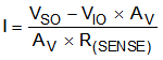
The SO pin on the DRV870x-Q1 device outputs an analog voltage equal to the voltage across the SP and SN pins multiplied by AV. The SO voltage is only valid for forward or reverse drive. Use Equation 2 to calculate the approximate current for the H-bridge.
When the SP and SN voltages are 0 V, the SO pin outputs the amplifier offset voltage times the amplifier gain, Vio × Av. When SP minus SN is greater than 0 V, the SO pin outputs the sum of the amplifier offset voltage and the sense resist or voltage, times the amplifier gain, (Vio + Vrsense) × Av. No capacitor is required on the SO pin.
 Figure 7-6 Current Sense Amplifier Output
If the voltage across the SP and SN pins exceeds 1 V, then the DRV870x-Q1 device flags an overcurrent condition.
The SO pin can source up to 5 mA of current. If the pin is shorted to ground, or if this pin drives a higher current load, the output functions as a constant-current source. The output voltage is not representative of the H-bridge current in this state.
 Figure 7-7 Current Sense Amplifier and Current Chopping Operation
During brake mode (slow decay), current is circulated through the low-side FETs. Because current is not flowing through the sense resistor, the SO pin does not represent the motor current.