SLVSEA2D August   2020  – April 2024 DRV8714-Q1 , DRV8718-Q1

PRODMIX  

  1.   1
  2. Features
  3. Applications
  4. Description
  5. Device Comparison Table
  6. Pin Configuration and Functions
    1. 5.1 VQFN (RVJ) 56-Pin Package and Pin Functions
    2. 5.2 VQFN (RHA) 40-Pin Package and Pin Functions
    3. 5.3 HTQFP (PHP) 48-Pin Package and Pin Functions
  7. Specifications
    1. 6.1 Absolute Maximum Ratings
    2. 6.2 ESD Ratings
    3. 6.3 Recommended Operating Conditions
    4. 6.4 Thermal Information
    5. 6.5 Electrical Characteristics
    6. 6.6 Timing Requirements
    7. 6.7 Timing Diagrams
    8. 6.8 Typical Characteristics
  8. Detailed Description
    1. 7.1 Overview
    2. 7.2 Functional Block Diagram
    3. 7.3 Feature Description
      1. 7.3.1 External Components
      2. 7.3.2 Device Interface Variants
        1. 7.3.2.1 Serial Peripheral Interface (SPI)
        2. 7.3.2.2 Hardware (H/W)
      3. 7.3.3 Input PWM Control Modes
        1. 7.3.3.1 Half-Bridge Control Scheme With Input PWM Mapping
          1. 7.3.3.1.1 DRV8718-Q1 Half-Bridge Control
          2. 7.3.3.1.2 DRV8714-Q1 Half-Bridge Control
        2. 7.3.3.2 H-Bridge Control
          1. 7.3.3.2.1 DRV8714-Q1 H-Bridge Control
        3. 7.3.3.3 Split HS and LS Solenoid Control
          1. 7.3.3.3.1 DRV8714-Q1 Split HS and LS Solenoid Control
      4. 7.3.4 Smart Gate Driver
        1. 7.3.4.1 Functional Block Diagram
        2. 7.3.4.2 Slew Rate Control (IDRIVE)
        3. 7.3.4.3 Gate Drive State Machine (TDRIVE)
        4. 7.3.4.4 Propagation Delay Reduction (PDR)
          1. 7.3.4.4.1 PDR Pre-Charge/Pre-Discharge Control Loop Operation Details
            1. 7.3.4.4.1.1 PDR Pre-Charge/Pre-Discharge Setup
          2. 7.3.4.4.2 PDR Post-Charge/Post-Discharge Control Loop Operation Details
            1. 7.3.4.4.2.1 PDR Post-Charge/Post-Discharge Setup
          3. 7.3.4.4.3 Detecting Drive and Freewheel MOSFET
        5. 7.3.4.5 Automatic Duty Cycle Compensation (DCC)
        6. 7.3.4.6 Closed Loop Slew Time Control (STC)
          1. 7.3.4.6.1 STC Control Loop Setup
      5. 7.3.5 Tripler (Dual-Stage) Charge Pump
      6. 7.3.6 Wide Common-Mode Current Shunt Amplifiers
      7. 7.3.7 Pin Diagrams
        1. 7.3.7.1 Logic Level Input Pin (INx/ENx, INx/PHx, nSLEEP, nSCS, SCLK, SDI)
        2. 7.3.7.2 Logic Level Push Pull Output (SDO)
        3. 7.3.7.3 Logic Level Multi-Function Pin (DRVOFF/nFLT)
        4. 7.3.7.4 Quad-Level Input (GAIN, MODE)
        5. 7.3.7.5 Six-Level Input (IDRIVE, VDS)
      8. 7.3.8 Protection and Diagnostics
        1. 7.3.8.1  Gate Driver Disable (DRVOFF/nFLT and EN_DRV)
        2. 7.3.8.2  Low IQ Powered Off Braking (POB, BRAKE)
        3. 7.3.8.3  Fault Reset (CLR_FLT)
        4. 7.3.8.4  DVDD Logic Supply Power on Reset (DVDD_POR)
        5. 7.3.8.5  PVDD Supply Undervoltage Monitor (PVDD_UV)
        6. 7.3.8.6  PVDD Supply Overvoltage Monitor (PVDD_OV)
        7. 7.3.8.7  VCP Charge Pump Undervoltage Lockout (VCP_UV)
        8. 7.3.8.8  MOSFET VDS Overcurrent Protection (VDS_OCP)
        9. 7.3.8.9  Gate Driver Fault (VGS_GDF)
        10. 7.3.8.10 Thermal Warning (OTW)
        11. 7.3.8.11 Thermal Shutdown (OTSD)
        12. 7.3.8.12 Offline Short Circuit and Open Load Detection (OOL and OSC)
        13. 7.3.8.13 Watchdog Timer
        14. 7.3.8.14 Fault Detection and Response Summary Table
    4. 7.4 Device Functional Modes
      1. 7.4.1 Inactive or Sleep State
      2. 7.4.2 Standby State
      3. 7.4.3 Operating State
    5. 7.5 Programming
      1. 7.5.1 SPI Interface
      2. 7.5.2 SPI Format
      3. 7.5.3 SPI Interface for Multiple Slaves
        1. 7.5.3.1 SPI Interface for Multiple Slaves in Daisy Chain
  9. Register Maps
    1. 8.1 DRV8718-Q1 Register Map
    2. 8.2 DRV8714-Q1 Register Map
    3. 8.3 DRV8718-Q1 Register Descriptions
      1. 8.3.1 DRV8718-Q1_STATUS Registers
      2. 8.3.2 DRV8718-Q1_CONTROL Registers
      3. 8.3.3 DRV8718-Q1_CONTROL_ADV Registers
      4. 8.3.4 DRV8718-Q1_STATUS_ADV Registers
    4. 8.4 DRV8714-Q1 Register Descriptions
      1. 8.4.1 DRV8714-Q1_STATUS Registers
      2. 8.4.2 DRV8714-Q1_CONTROL Registers
      3. 8.4.3 DRV8714-Q1_CONTROL_ADV Registers
      4. 8.4.4 DRV8714-Q1_STATUS_ADV Registers
  10. Application Implementation
    1. 9.1 Application Information
    2. 9.2 Typical Application
      1. 9.2.1 Design Requirements
      2. 9.2.2 Detailed Design Procedure
        1. 9.2.2.1 Gate Driver Configuration
          1. 9.2.2.1.1 VCP Load Calculation Example
          2. 9.2.2.1.2 IDRIVE Calculation Example
          3. 9.2.2.1.3 tDRIVE Calculation Example
          4. 9.2.2.1.4 Maximum PWM Switching Frequency
        2. 9.2.2.2 Current Shunt Amplifier Configuration
        3. 9.2.2.3 Power Dissipation
      3. 9.2.3 Application Curves
    3. 9.3 Initialization
    4. 9.4 Power Supply Recommendations
      1. 9.4.1 Bulk Capacitance Sizing
    5. 9.5 Layout
      1. 9.5.1 Layout Guidelines
      2. 9.5.2 Layout Example
  11. 10Device Documentation and Support
    1. 10.1 Documentation Support
      1. 10.1.1 Related Documents
    2. 10.2 Receiving Notification of Documentation Updates
    3. 10.3 Support Resources
    4. 10.4 Trademarks
    5. 10.5 Electrostatic Discharge Caution
    6. 10.6 Glossary
  12. 11Revision History
  13. 12Mechanical, Packaging, and Orderable Information
    1. 12.1 Package Option Addendum

Package Options

Mechanical Data (Package|Pins)
Thermal pad, mechanical data (Package|Pins)
Orderable Information

Description

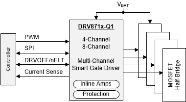
The DRV871x-Q1 family of devices are highly integrated, multi-channel gate drivers intended for driving multiple motors or loads. The devices integrate either 4 (DRV8714-Q1) or 8 (DRV8718-Q1) half-bridge gate drivers, driver power supplies, current shunt amplifiers, and protection monitors reducing total system complexity, size, and cost.

A smart gate drive architecture manages dead time to prevent shoot-through, controls slew rate to decrease electromagnetic interference (EMI), and optimizes propagation delay for enhanced performance.

Input modes are provided for independent half-bridge or H-bridge control. Four PWM inputs can be multiplexed between the different drivers in combination with SPI control.

Wide common mode shunt amplifiers provide inline current sensing to continuously measure motor current even during recirculating windows. The amplifier can be used in low-side or high-side sense configurations if inline sensing is not required.

The devices provide an array of protection features to promote robust system operation. These include under and overvoltage monitors, VDS overcurrent and VGS gate fault monitors for the external MOSFETs, offline open load and short circuit diagnostics, and internal thermal warning and shutdown protection.

Device Information(1)
PART NUMBER PACKAGE BODY SIZE (NOM)
DRV8714-Q1 VQFN (40) 6.00mm x 6.00mm
HTQFP (48) 7.00mm x 7.00mm
VQFN (56) 8.00mm x 8.00mm
DRV8718-Q1 VQFN (56) 8.00mm x 8.00mm
For all available packages, see the orderable addendum at the end of the data sheet.
GUID-0B3A9998-5689-4E6E-B0BF-7E7129E0E59E-low.gif Simple Block Diagram