SLVSEA2D August   2020  – April 2024 DRV8714-Q1 , DRV8718-Q1

PRODMIX  

  1.   1
  2. Features
  3. Applications
  4. Description
  5. Device Comparison Table
  6. Pin Configuration and Functions
    1. 5.1 VQFN (RVJ) 56-Pin Package and Pin Functions
    2. 5.2 VQFN (RHA) 40-Pin Package and Pin Functions
    3. 5.3 HTQFP (PHP) 48-Pin Package and Pin Functions
  7. Specifications
    1. 6.1 Absolute Maximum Ratings
    2. 6.2 ESD Ratings
    3. 6.3 Recommended Operating Conditions
    4. 6.4 Thermal Information
    5. 6.5 Electrical Characteristics
    6. 6.6 Timing Requirements
    7. 6.7 Timing Diagrams
    8. 6.8 Typical Characteristics
  8. Detailed Description
    1. 7.1 Overview
    2. 7.2 Functional Block Diagram
    3. 7.3 Feature Description
      1. 7.3.1 External Components
      2. 7.3.2 Device Interface Variants
        1. 7.3.2.1 Serial Peripheral Interface (SPI)
        2. 7.3.2.2 Hardware (H/W)
      3. 7.3.3 Input PWM Control Modes
        1. 7.3.3.1 Half-Bridge Control Scheme With Input PWM Mapping
          1. 7.3.3.1.1 DRV8718-Q1 Half-Bridge Control
          2. 7.3.3.1.2 DRV8714-Q1 Half-Bridge Control
        2. 7.3.3.2 H-Bridge Control
          1. 7.3.3.2.1 DRV8714-Q1 H-Bridge Control
        3. 7.3.3.3 Split HS and LS Solenoid Control
          1. 7.3.3.3.1 DRV8714-Q1 Split HS and LS Solenoid Control
      4. 7.3.4 Smart Gate Driver
        1. 7.3.4.1 Functional Block Diagram
        2. 7.3.4.2 Slew Rate Control (IDRIVE)
        3. 7.3.4.3 Gate Drive State Machine (TDRIVE)
        4. 7.3.4.4 Propagation Delay Reduction (PDR)
          1. 7.3.4.4.1 PDR Pre-Charge/Pre-Discharge Control Loop Operation Details
            1. 7.3.4.4.1.1 PDR Pre-Charge/Pre-Discharge Setup
          2. 7.3.4.4.2 PDR Post-Charge/Post-Discharge Control Loop Operation Details
            1. 7.3.4.4.2.1 PDR Post-Charge/Post-Discharge Setup
          3. 7.3.4.4.3 Detecting Drive and Freewheel MOSFET
        5. 7.3.4.5 Automatic Duty Cycle Compensation (DCC)
        6. 7.3.4.6 Closed Loop Slew Time Control (STC)
          1. 7.3.4.6.1 STC Control Loop Setup
      5. 7.3.5 Tripler (Dual-Stage) Charge Pump
      6. 7.3.6 Wide Common-Mode Current Shunt Amplifiers
      7. 7.3.7 Pin Diagrams
        1. 7.3.7.1 Logic Level Input Pin (INx/ENx, INx/PHx, nSLEEP, nSCS, SCLK, SDI)
        2. 7.3.7.2 Logic Level Push Pull Output (SDO)
        3. 7.3.7.3 Logic Level Multi-Function Pin (DRVOFF/nFLT)
        4. 7.3.7.4 Quad-Level Input (GAIN, MODE)
        5. 7.3.7.5 Six-Level Input (IDRIVE, VDS)
      8. 7.3.8 Protection and Diagnostics
        1. 7.3.8.1  Gate Driver Disable (DRVOFF/nFLT and EN_DRV)
        2. 7.3.8.2  Low IQ Powered Off Braking (POB, BRAKE)
        3. 7.3.8.3  Fault Reset (CLR_FLT)
        4. 7.3.8.4  DVDD Logic Supply Power on Reset (DVDD_POR)
        5. 7.3.8.5  PVDD Supply Undervoltage Monitor (PVDD_UV)
        6. 7.3.8.6  PVDD Supply Overvoltage Monitor (PVDD_OV)
        7. 7.3.8.7  VCP Charge Pump Undervoltage Lockout (VCP_UV)
        8. 7.3.8.8  MOSFET VDS Overcurrent Protection (VDS_OCP)
        9. 7.3.8.9  Gate Driver Fault (VGS_GDF)
        10. 7.3.8.10 Thermal Warning (OTW)
        11. 7.3.8.11 Thermal Shutdown (OTSD)
        12. 7.3.8.12 Offline Short Circuit and Open Load Detection (OOL and OSC)
        13. 7.3.8.13 Watchdog Timer
        14. 7.3.8.14 Fault Detection and Response Summary Table
    4. 7.4 Device Functional Modes
      1. 7.4.1 Inactive or Sleep State
      2. 7.4.2 Standby State
      3. 7.4.3 Operating State
    5. 7.5 Programming
      1. 7.5.1 SPI Interface
      2. 7.5.2 SPI Format
      3. 7.5.3 SPI Interface for Multiple Slaves
        1. 7.5.3.1 SPI Interface for Multiple Slaves in Daisy Chain
  9. Register Maps
    1. 8.1 DRV8718-Q1 Register Map
    2. 8.2 DRV8714-Q1 Register Map
    3. 8.3 DRV8718-Q1 Register Descriptions
      1. 8.3.1 DRV8718-Q1_STATUS Registers
      2. 8.3.2 DRV8718-Q1_CONTROL Registers
      3. 8.3.3 DRV8718-Q1_CONTROL_ADV Registers
      4. 8.3.4 DRV8718-Q1_STATUS_ADV Registers
    4. 8.4 DRV8714-Q1 Register Descriptions
      1. 8.4.1 DRV8714-Q1_STATUS Registers
      2. 8.4.2 DRV8714-Q1_CONTROL Registers
      3. 8.4.3 DRV8714-Q1_CONTROL_ADV Registers
      4. 8.4.4 DRV8714-Q1_STATUS_ADV Registers
  10. Application Implementation
    1. 9.1 Application Information
    2. 9.2 Typical Application
      1. 9.2.1 Design Requirements
      2. 9.2.2 Detailed Design Procedure
        1. 9.2.2.1 Gate Driver Configuration
          1. 9.2.2.1.1 VCP Load Calculation Example
          2. 9.2.2.1.2 IDRIVE Calculation Example
          3. 9.2.2.1.3 tDRIVE Calculation Example
          4. 9.2.2.1.4 Maximum PWM Switching Frequency
        2. 9.2.2.2 Current Shunt Amplifier Configuration
        3. 9.2.2.3 Power Dissipation
      3. 9.2.3 Application Curves
    3. 9.3 Initialization
    4. 9.4 Power Supply Recommendations
      1. 9.4.1 Bulk Capacitance Sizing
    5. 9.5 Layout
      1. 9.5.1 Layout Guidelines
      2. 9.5.2 Layout Example
  11. 10Device Documentation and Support
    1. 10.1 Documentation Support
      1. 10.1.1 Related Documents
    2. 10.2 Receiving Notification of Documentation Updates
    3. 10.3 Support Resources
    4. 10.4 Trademarks
    5. 10.5 Electrostatic Discharge Caution
    6. 10.6 Glossary
  12. 11Revision History
  13. 12Mechanical, Packaging, and Orderable Information
    1. 12.1 Package Option Addendum

Package Options

Mechanical Data (Package|Pins)
Thermal pad, mechanical data (Package|Pins)
Orderable Information

Functional Block Diagram

Figure 7-11 shows a high level function block diagram for the half-bridge gate driver architecture. The gate driver blocks provide a variety of functions for MOSFET control, feedback, and protection. This includes complimentary, push-pull high-side and low-side gate drivers with adjustable drive currents, control logic level shifters, VDS, VGS, and VSH (switch-node) feedback comparators, a high-side Zener clamp, plus passive and active pulldown resistors.
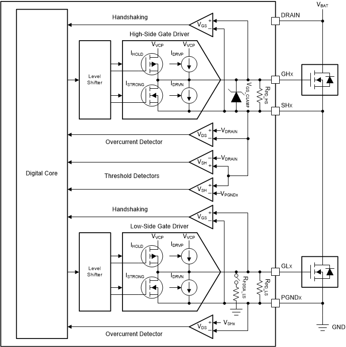
GUID-995EA3E9-332D-4629-8E5E-532AD476DD25-low.gifFigure 7-11 Gate Driver Functional Block Diagram