SLVSAS7D February   2011  – March 2021 DRV8801-Q1

PRODUCTION DATA  

  1. Features
  2. Applications
  3. Description
  4. Revision History
  5. Pin Configuration and Functions
  6. Specifications
    1. 6.1 Absolute Maximum Ratings
    2. 6.2 ESD Ratings
    3. 6.3 Recommended Operating Conditions
    4. 6.4 Thermal Information
    5. 6.5 Electrical Characteristics
    6. 6.6 Timing Requirements
    7. 6.7 Typical Characteristics
  7. Detailed Description
    1. 7.1 Overview
    2. 7.2 Functional Block Diagram
    3. 7.3 Feature Description
      1. 7.3.1 Power Supervisor
      2. 7.3.2 Bridge Control
        1. 7.3.2.1 MODE 1
        2. 7.3.2.2 MODE 2
      3. 7.3.3 Fast Decay with Synchronous Rectification
      4. 7.3.4 Slow Decay with Synchronous Rectification (Brake Mode)
      5. 7.3.5 Charge Pump
      6. 7.3.6 SENSE
      7. 7.3.7 VPROPI
        1. 7.3.7.1 Connecting VPROPI Output to ADC
      8. 7.3.8 Protection Circuits
        1. 7.3.8.1 VBB Undervoltage Lockout (UVLO)
        2. 7.3.8.2 Overcurrent Protection (OCP)
        3. 7.3.8.3 Overtemperature Warning (OTW)
        4. 7.3.8.4 Overtemperature Shutdown (OTS)
      9. 7.3.9 Thermal Shutdown (TSD)
    4. 7.4 Device Functional Modes
  8. Application and Implementation
    1. 8.1 Application Information
    2. 8.2 Typical Application
      1. 8.2.1 Design Requirements
      2. 8.2.2 Detailed Design Procedure
        1. 8.2.2.1 Motor Voltage
        2. 8.2.2.2 Power Dissipation
        3. 8.2.2.3 Thermal Considerations
          1. 8.2.2.3.1 Junction-to-Ambiant Thermal Impedance (ƟJA)
        4. 8.2.2.4 Motor Current Trip Point
        5. 8.2.2.5 Sense Resistor Selection
        6. 8.2.2.6 Drive Current
      3. 8.2.3 Pulse-Width Modulating
        1. 8.2.3.1 Pulse-Width Modulating ENABLE
        2. 8.2.3.2 Pulse-Width Modulating PHASE
      4. 8.2.4 Application Curves
    3. 8.3 Parallel Configuration
      1. 8.3.1 Parallel Connections
      2. 8.3.2 Non – Parallel Connections
      3. 8.3.3 Wiring nFAULT as Wired OR
      4. 8.3.4 Electrical Considerations
        1. 8.3.4.1 Device Spacing
        2. 8.3.4.2 Recirculation Current Handling
        3. 8.3.4.3 Sense Resistor Selection
        4. 8.3.4.4 Maximum System Current
  9. Power Supply Recommendations
    1. 9.1 Bulk Capacitance
  10. 10Layout
    1. 10.1 Layout Guidelines
    2. 10.2 Layout Example
  11. 11Device and Documentation Support
    1. 11.1 Documentation Support
      1. 11.1.1 Related Documentation
    2. 11.2 Receiving Notification of Documentation Updates
    3. 11.3 Support Resources
    4. 11.4 Trademarks
    5. 11.5 Electrostatic Discharge Caution
    6. 11.6 Glossary
  12. 12Mechanical, Packaging, and Orderable Information

Package Options

Mechanical Data (Package|Pins)
Thermal pad, mechanical data (Package|Pins)
Orderable Information

Timing Requirements

MINNOMMAXUNIT
tpdPropagation delay timeInput edge to source or sink ON600ns
Input edge to source or sink OFF100
tCODCrossover delay500ns
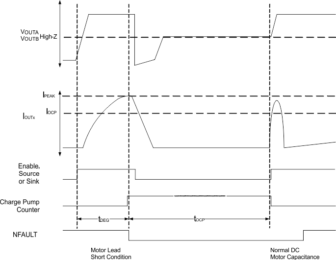
tDEGOvercurrent deglitch time3µs
tOCPOvercurrent retry time1.2ms
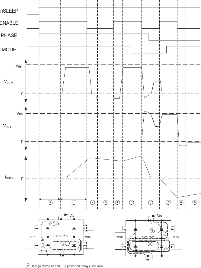
GUID-20210128-CA0I-PKKH-KM36-TXHTNL2955KH-low.gif Figure 6-1 PWM Control Timing
GUID-27E305CE-D22D-40EB-AFB8-E529E27567A3-low.gifFigure 6-2 Overcurrent Control Timing