SLVSAX9E September 2011 – January 2016 DRV8818
PRODUCTION DATA.
- 1 Features
- 2 Applications
- 3 Description
- 4 Revision History
- 5 Pin Configuration and Functions
- 6 Specifications
- 7 Detailed Description
- 8 Application and Implementation
- 9 Power Supply Recommendations
- 10Layout
- 11Device and Documentation Support
- 12Mechanical, Packaging, and Orderable Information
Package Options
Mechanical Data (Package|Pins)
- PWP|28
Thermal pad, mechanical data (Package|Pins)
- PWP|28
Orderable Information
6 Specifications
6.1 Absolute Maximum Ratings
over operating free-air temperature range (unless otherwise noted)(1) (2) (3)| MIN | MAX | UNIT | |||
|---|---|---|---|---|---|
| VMX | Power supply voltage | –0.3 | 35 | V | |
| VCC | Power supply voltage | –0.3 | 7 | V | |
| Digital pin voltage | –0.5 | 7 | V | ||
| VREF | Input voltage | 0 | VCC | V | |
| ISENSEx(4) | Pin voltage | –0.875 | 0.875 | V | |
| IO(peak) | Peak motor drive output current | Internally limited | |||
| PD | Continuous total power dissipation | See Thermal Information | |||
| TJ | Operating junction temperature | –40 | 150 | °C | |
| Tstg | Storage temperature | –60 | 150 | °C | |
(1) Stresses beyond those listed under Absolute Maximum Ratings may cause permanent damage to the device. These are stress ratings only, and functional operation of the device at these or any other conditions beyond those indicated under Recommended Operating Conditions is not implied. Exposure to absolute-maximum-rated conditions for extended periods may affect device reliability.
(2) All voltage values are with respect to network ground terminal.
(3) Power dissipation and thermal limits must be observed.
(4) Transients of ±1V for less than 25ns are acceptable.
6.2 ESD Ratings
| VALUE | UNIT | ||||
|---|---|---|---|---|---|
| V(ESD) | Electrostatic discharge | Human body model (HBM), per ANSI/ESDA/JEDEC JS-001, all pins(1) | ±4000 | V | |
| Charged device model (CDM), per JEDEC specification JESD22-C101, all pins(2) | ±1000 | ||||
(1) JEDEC document JEP155 states that 500-V HBM allows safe manufacturing with a standard ESD control process.
(2) JEDEC document JEP157 states that 250-V CDM allows safe manufacturing with a standard ESD control process.
6.3 Recommended Operating Conditions
TA = 25°C (unless otherwise noted)| MIN | NOM | MAX | UNIT | ||
|---|---|---|---|---|---|
| VM | Motor power supply voltage(1) | 8 | 35 | V | |
| VCC | Logic power supply voltage | 3 | 5.5 | V | |
| VREF | VREF input voltage | 0 | VCC | V | |
| RX | RX resistance value | 12 | 56 | 100 | kΩ |
| CX | CX capacitance value | 470 | 680 | 1500 | pF |
(1) All VM pins must be connected to the same supply voltage.
6.4 Thermal Information
| THERMAL METRIC(1) | DRV8818 | UNIT | |
|---|---|---|---|
| PWP (HTSSOP) | |||
| 28 PINS | |||
| RθJA | Junction-to-ambient thermal resistance | 32.2 | °C/W |
| RθJC(top) | Junction-to-case (top) thermal resistance | 16.3 | °C/W |
| RθJB | Junction-to-board thermal resistance | 14 | °C/W |
| ψJT | Junction-to-top characterization parameter | 0.5 | °C/W |
| ψJB | Junction-to-board characterization parameter | 13.8 | °C/W |
| RθJC(bot) | Junction-to-case (bottom) thermal resistance | 2.1 | °C/W |
(1) For more information about traditional and new thermal metrics, see the Semiconductor and IC Package Thermal Metrics application report, SPRA953.
6.5 Electrical Characteristics
TA = 25°C (unless otherwise noted)6.6 Timing Requirements
TA = 25°C (unless otherwise noted)| MIN | NOM | MAX | UNIT | ||||
|---|---|---|---|---|---|---|---|
| 1 | fSTEP | Step frequency | 500 | kHz | |||
| 2 | tWH(STEP) | Pulse duration, STEP high | 1 | μs | |||
| 3 | tWL(STEP) | Pulse duration, STEP low | 1 | μs | |||
| 4 | tSU(STEP) | Setup time, command before STEP rising | 200 | ns | |||
| 5 | tH(STEP) | Hold time, command after STEP rising | 200 | ns | |||
| 6 | tWAKE | Wakeup time, SLEEPn inactive high to STEP input accepted | 1 | ms | |||
| 7 | tSLEEP | Sleep time, SLEEPn active low to outputs disabled | 5 | μs | |||
| 8 | tENABLE | Enable time, ENABLEn inactive high to outputs enabled | 20 | μs | |||
| 9 | tDISABLE | Disable time, ENABLEn active low to outputs disabled | 20 | μs | |||
| 10 | tRESETR | Reset release time, RESETn inactive high to outputs enabled | 5 | μs | |||
| 11 | tRESET | Reset time, RESETn active low to outputs disabled | 5 | μs | |||
6.7 Motor Driver Timing Switching Characteristics
TA = 25°C (unless otherwise noted)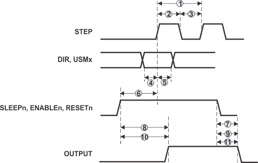 Figure 1. Timing Diagram
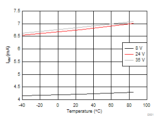
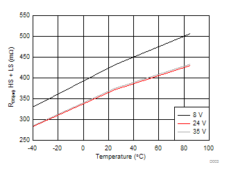
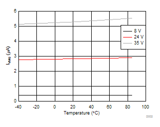
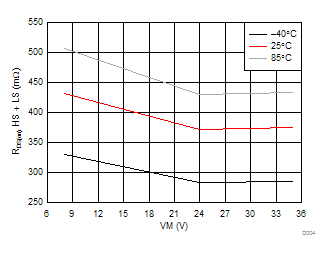
6.8 Typical Characteristics
