SLVSDY7B October 2017 – January 2021 DRV8873-Q1
PRODUCTION DATA
- 1 Features
- 2 Applications
- 3 Description
- 4 Revision History
- 5 Pin Configuration and Functions
- 6 Specifications
-
7 Detailed Description
- 7.1 Overview
- 7.2 Functional Block Diagram
- 7.3 Feature Description
- 7.4 Device Functional Modes
- 7.5 Programming
- 7.6 Register Maps
- 8 Application and Implementation
- 9 Power Supply Recommendations
- 10Layout
- 11Device and Documentation Support
- 12Mechanical, Packaging, and Orderable Information
Package Options
Mechanical Data (Package|Pins)
- PWP|24
Thermal pad, mechanical data (Package|Pins)
- PWP|24
Orderable Information
7.3.1.5 Slew-Rate Control
The rise and fall times (tr and tf) of the outputs can be adjusted on the hardware version of the device by changing the value of an external resistor connected from the SR pin to ground. On the SPI version of the device, the slew rate can be adjusted through the SPI. The output slew rate is adjusted internally to the device by controlling the ramp rate of the driven FET gate. The voltage or resistance on the SR pin sets the output rise and fall times in the hardware version of the device.
| CONNECTION | SR | CIRCUIT |
|---|---|---|
| Connect to GND | 53.2 V/µs | 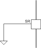 |
| 22 kΩ ± 5% to GND | 34 V/µs | 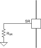 |
| 68 kΩ ± 5% to GND | 18.3 V/µs | |
| > 2 MΩ to GND (Hi-Z) | 13 V/µs | 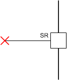 |
| 51 kΩ ± 5% to DVDD | 7.9 V/µs | 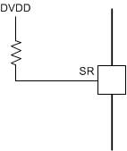 |
| Connect to DVDD | 2.6 V/µs | 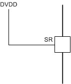 |
Figure 7-8 shows the internal circuit block for the SR pin.
 Figure 7-8 SR Block Diagram
Table 7-11 lists the settings in the SPI register that set the output rise and fall times in the SPI version of the device.
| SR | RISE TIME (V/µs) | FALL TIME (V/µs) |
|---|---|---|
| 000b | 53.2 | 53.2 |
| 001b | 34 | 34 |
| 010b | 18.3 | 18.3 |
| 011b | 13 | 13 |
| 100b | 10.8 | 10.8 |
| 101b | 7.9 | 7.9 |
| 110b | 5.3 | 5.3 |
| 111b | 2.6 | 2.6 |
The typical voltage on the SR pin is 3 V and is driven internally. Changing the resistor value on the SR pin changes the slew-rate setting from approximately 2.6 V/µs to 53.2 V/µs. The recommended values for the external resistor are shown in the Section 7.3.3.2 section. If the SR pin is grounded then the slew rate is 53.2 V/µs. Leaving the SR pin as a no-connect pin sets the slew rate to 13 V/µs. Tying it to the DVDD pin sets the slew rate to 2.6 V/µs.