SLVSET1 August   2018 DRV8873

PRODUCTION DATA.  

  1. Features
  2. Applications
  3. Description
    1.     Simplified Schematic
  4. Revision History
  5. Pin Configuration and Functions
    1.     Pin Functions
  6. Specifications
    1. 6.1 Absolute Maximum Ratings
    2. 6.2 ESD Ratings
    3. 6.3 Recommended Operating Conditions
    4. 6.4 Thermal Information
    5. 6.5 Electrical Characteristics
    6. 6.6 SPI Timing Requirements
    7. 6.7 Typical Characteristics
  7. Detailed Description
    1. 7.1 Overview
    2. 7.2 Functional Block Diagram
    3. 7.3 Feature Description
      1. 7.3.1 Bridge Control
        1. 7.3.1.1 Control Modes
        2. 7.3.1.2 Half-Bridge Operation
        3. 7.3.1.3 Internal Current Sense and Current Regulation
        4. 7.3.1.4 Slew-Rate Control
        5. 7.3.1.5 Dead Time
        6. 7.3.1.6 Propagation Delay
        7. 7.3.1.7 nFAULT Pin
        8. 7.3.1.8 nSLEEP as SDO Reference
      2. 7.3.2 Motor Driver Protection Circuits
        1. 7.3.2.1 VM Undervoltage Lockout (UVLO)
        2. 7.3.2.2 VCP Undervoltage Lockout (CPUV)
        3. 7.3.2.3 Overcurrent Protection (OCP)
          1. 7.3.2.3.1 Latched Shutdown (OCP_MODE = 00b)
          2. 7.3.2.3.2 Automatic Retry (OCP_MODE = 01b)
          3. 7.3.2.3.3 Report Only (OCP_MODE = 10b)
          4. 7.3.2.3.4 Disabled (OCP_MODE = 11b)
        4. 7.3.2.4 Open-Load Detection (OLD)
          1. 7.3.2.4.1 Open-Load Detection in Passive Mode (OLP)
          2. 7.3.2.4.2 Open-Load Detection in Active Mode (OLA)
        5. 7.3.2.5 Thermal Shutdown (TSD)
          1. 7.3.2.5.1 Latched Shutdown (TSD_MODE = 0b)
          2. 7.3.2.5.2 Automatic Recovery (TSD_MODE = 1b)
        6. 7.3.2.6 Thermal Warning (OTW)
      3. 7.3.3 Hardware Interface
        1. 7.3.3.1 MODE (Tri-Level Input)
        2. 7.3.3.2 Slew Rate
    4. 7.4 Device Functional Modes
      1. 7.4.1 Motor Driver Functional Modes
        1. 7.4.1.1 Sleep Mode (nSLEEP = 0)
        2. 7.4.1.2 Disable Mode (nSLEEP = 1, DISABLE = 1)
        3. 7.4.1.3 Operating Mode (nSLEEP = 1, DISABLE = 0)
        4. 7.4.1.4 nSLEEP Reset Pulse
    5. 7.5 Programming
      1. 7.5.1 Serial Peripheral Interface (SPI) Communication
        1. 7.5.1.1 SPI Format
        2. 7.5.1.2 SPI for a Single Slave Device
        3. 7.5.1.3 SPI for Multiple Slave Devices in Parallel Configuration
        4. 7.5.1.4 SPI for Multiple Slave Devices in Daisy Chain Configuration
    6. 7.6 Register Maps
      1. 7.6.1 Status Registers
        1. 7.6.1.1 FAULT Status Register Name (address = 0x00)
          1. Table 21. FAULT Status Register Field Descriptions
        2. 7.6.1.2 DIAG Status Register Name (address = 0x01)
          1. Table 22. DIAG Status Register Field Descriptions
      2. 7.6.2 Control Registers
        1. 7.6.2.1 IC1 Control Register (address = 0x02)
          1. Table 24. IC1 Control Register Field Descriptions
        2. 7.6.2.2 IC2 Control Register (address = 0x03)
          1. Table 25. IC2 Control Register Field Descriptions
        3. 7.6.2.3 IC3 Control Register (address = 0x04)
          1. Table 26. IC3 Control Register Field Descriptions
        4. 7.6.2.4 IC4 Control Register (address = 0x05)
          1. Table 27. IC4 Control Register Field Descriptions
  8. Application and Implementation
    1. 8.1 Application Information
    2. 8.2 Typical Application
      1. 8.2.1 Design Requirements
        1. 8.2.1.1 Motor Voltage
        2. 8.2.1.2 Drive Current and Power Dissipation
        3. 8.2.1.3 Sense Resistor
      2. 8.2.2 Detailed Design Procedure
        1. 8.2.2.1 Thermal Considerations
        2. 8.2.2.2 Heatsinking
      3. 8.2.3 Application Curves
  9. Power Supply Recommendations
    1. 9.1 Bulk Capacitance Sizing
  10. 10Layout
    1. 10.1 Layout Guidelines
    2. 10.2 Layout Example
  11. 11Device and Documentation Support
    1. 11.1 Documentation Support
      1. 11.1.1 Related Documentation
    2. 11.2 Receiving Notification of Documentation Updates
    3. 11.3 Community Resources
    4. 11.4 Trademarks
    5. 11.5 Electrostatic Discharge Caution
    6. 11.6 Glossary
  12. 12Mechanical, Packaging, and Orderable Information
    1. 12.1 Package Option Addendum
      1. 12.1.1 Packaging Information
      2. 12.1.2 Tape and Reel Information

Package Options

Mechanical Data (Package|Pins)
Thermal pad, mechanical data (Package|Pins)
Orderable Information

Half-Bridge Operation

The device can be used to drive two solenoids or unidirectional brushed DC-motor loads instead of a brushed-DC motor in full H-bridge configuration. Independent half-bridge control is preferred for operation in this mode; however, using the PH/EN or PWM modes is not restricted if the correct driving and braking states can be achieved.
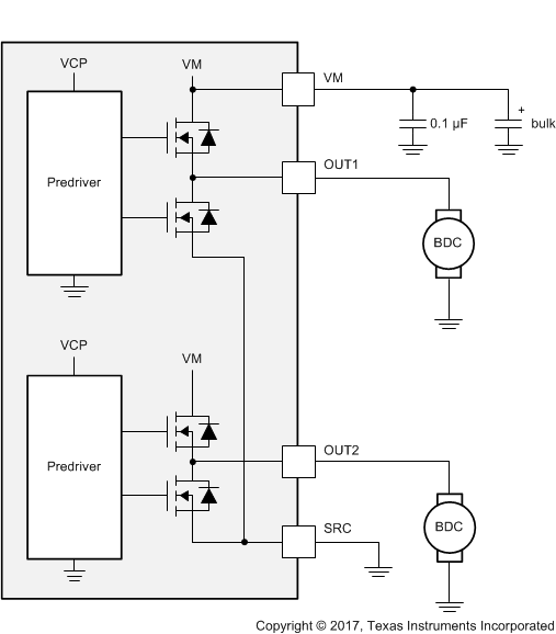
DRV8873 drv8873q1_independant_half_bridge_m.gifFigure 11. Independent Half bridge Mode Driving Two Low-Side Loads

TI does not recommend tying the OUT1 and OUT2 pins together and drive a load. The half bridges may be out of synchronization in this configuration and any mismatch in the input commands can momentarily result in shoot through condition. This mismatch can be mitigated by adding an inductor in-line with the outputs.

If loads are connected between the OUTx and VM pins, the device can draw more current than specified in the Electrical Characteristics table. To avoid this condition, TI recommends connecting loads in the configuration shown in Figure 11.

Depending on how the loads are connected on the outputs pin, some of the features offered by the device could have reduced functionality. For example, having a load between the OUTx and GND pins, as shown in Figure 11, results in false trips of the open-load diagnosis in active-mode (OLA). Having a load tied between the OUTx and VM pins restricts the use of internal current regulation because no means of measuring current flowing through the load with the current mirror block is available. Table 7 lists these use cases.

Table 7. Control Mode Configuration

LOAD CONNECTIONS FUNCTIONALITY
NODE 1 NODE 2 OLA CURRENT REGULATION (ITRIP)
OUTx GND Not Available Operational
OUTx VM Operational Not Available