SLVSD19A June   2015  – July 2015 DRV8881

PRODUCTION DATA.  

  1. Features
  2. Applications
  3. Description
    1.     Device Images
      1.      DRV8881E Simplified System Diagram
      2.      DRV8881P Simplified System Diagram
  4. Revision History
  5. Pin Configuration and Functions
    1.     Pin Functions
    2.     DRV8881E PH/EN Pin Functions
    3.     DRV8881P PWM Pin Functions
  6. Specifications
    1. 6.1 Absolute Maximum Ratings
    2. 6.2 ESD Ratings
    3. 6.3 Recommended Operating Conditions
    4. 6.4 Thermal Information
    5. 6.5 Electrical Characteristics
    6. 6.6 Typical Characteristics
  7. Detailed Description
    1. 7.1 Overview
    2. 7.2 Functional Block Diagrams
    3. 7.3 Feature Description
      1. 7.3.1  Motor Driver Current Ratings
        1. 7.3.1.1 Peak Current Rating
        2. 7.3.1.2 RMS Current Rating
        3. 7.3.1.3 Full-Scale Current Rating
      2. 7.3.2  PWM Motor Drivers
      3. 7.3.3  Bridge Control
      4. 7.3.4  Current Regulation
      5. 7.3.5  Decay Modes
        1. 7.3.5.1 Mode 1: Slow Decay
        2. 7.3.5.2 Mode 2: Fast Decay
        3. 7.3.5.3 Mode 3: 30%/70% Mixed Decay
      6. 7.3.6  Smart tune
      7. 7.3.7  Adaptive Blanking Time
      8. 7.3.8  Parallel Mode
      9. 7.3.9  Charge Pump
      10. 7.3.10 LDO Voltage Regulator
      11. 7.3.11 Logic and Tri-Level Pin Diagrams
      12. 7.3.12 Protection Circuits
        1. 7.3.12.1 VM Undervoltage Lockout (UVLO)
        2. 7.3.12.2 VCP UVLO (CPUV)
        3. 7.3.12.3 Overcurrent Protection (OCP)
        4. 7.3.12.4 Thermal Shutdown (TSD)
    4. 7.4 Device Functional Modes
  8. Application and Implementation
    1. 8.1 Application Information
    2. 8.2 Typical Applications
      1. 8.2.1 DRV8881P Typical Application
        1. 8.2.1.1 Design Requirements
        2. 8.2.1.2 Detailed Design Procedure
          1. 8.2.1.2.1 Current Regulation
          2. 8.2.1.2.2 Stepper Motor Speed
          3. 8.2.1.2.3 Decay Modes
          4. 8.2.1.2.4 Sense Resistor
        3. 8.2.1.3 Application Curve
      2. 8.2.2 Alternate Application
        1. 8.2.2.1 Design Requirements
        2. 8.2.2.2 Detailed Design Procedure
          1. 8.2.2.2.1 Current Regulation
        3. 8.2.2.3 Application Curves
  9. Power Supply Recommendations
    1. 9.1 Bulk Capacitance Sizing
  10. 10Layout
    1. 10.1 Layout Guidelines
    2. 10.2 Layout Example
  11. 11Device and Documentation Support
    1. 11.1 Documentation Support
      1. 11.1.1 Related Documentation
    2. 11.2 Community Resources
    3. 11.3 Trademarks
    4. 11.4 Electrostatic Discharge Caution
    5. 11.5 Glossary
  12. 12Mechanical, Packaging, and Orderable Information

Package Options

Mechanical Data (Package|Pins)
Thermal pad, mechanical data (Package|Pins)
Orderable Information

Mode 1: Slow Decay

To configure the DRV8881 into this mode, pull DECAY1 and DECAY0 logic low.
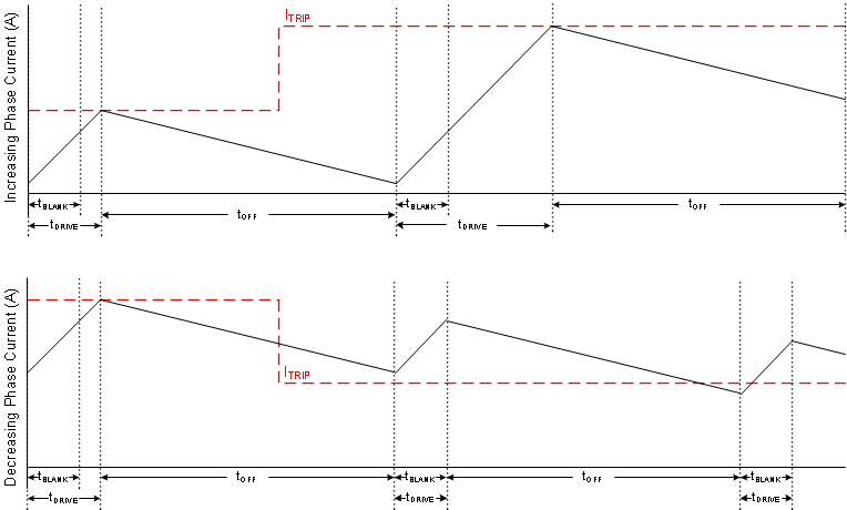
DRV8881 tim_slow_decay_lvsd19.gifFigure 16. Slow Decay Mode

During slow decay, both of the low-side FETs of the H-bridge are turned on, allowing the current to be recirculated.

Slow decay exhibits the least current ripple of the decay modes for a given tOFF. However, if the current trip level is decreasing, slow decay will take a long time to settle to the new ITRIP level because the current decreases very slowly.