SLVSD19A June 2015 – July 2015 DRV8881
PRODUCTION DATA.
- 1 Features
- 2 Applications
- 3 Description
- 4 Revision History
- 5 Pin Configuration and Functions
- 6 Specifications
-
7 Detailed Description
- 7.1 Overview
- 7.2 Functional Block Diagrams
- 7.3
Feature Description
- 7.3.1 Motor Driver Current Ratings
- 7.3.2 PWM Motor Drivers
- 7.3.3 Bridge Control
- 7.3.4 Current Regulation
- 7.3.5 Decay Modes
- 7.3.6 Smart tune
- 7.3.7 Adaptive Blanking Time
- 7.3.8 Parallel Mode
- 7.3.9 Charge Pump
- 7.3.10 LDO Voltage Regulator
- 7.3.11 Logic and Tri-Level Pin Diagrams
- 7.3.12 Protection Circuits
- 7.4 Device Functional Modes
- 8 Application and Implementation
- 9 Power Supply Recommendations
- 10Layout
- 11Device and Documentation Support
- 12Mechanical, Packaging, and Orderable Information
Package Options
Mechanical Data (Package|Pins)
Thermal pad, mechanical data (Package|Pins)
Orderable Information
5 Pin Configuration and Functions
PWP Package
28-Pin HTSSOP
Top View DRV8881E

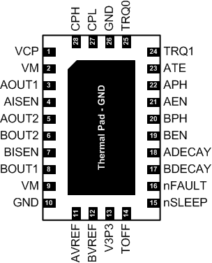
RHR Package
28-Pin WQFN
Top View DRV8881E

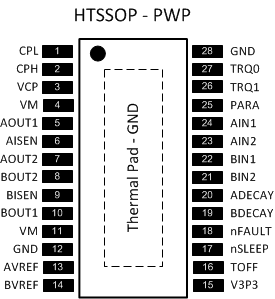
PWP Package
28-Pin HTSSOP
Top View DRV8881P

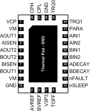
RHR Package
28-Pin WQFN
Top View DRV8881P

Pin Functions
| PIN | TYPE | DESCRIPTION | |||
|---|---|---|---|---|---|
| NAME | PWP | RHR | |||
| CPL | 1 | 27 | PWR | Charge pump output | Connect a VM rated, 0.1-µF ceramic capacitor between CPH and CPL |
| CPH | 2 | 28 | |||
| VCP | 3 | 1 | O | Charge pump output | Connect a 16-V, 0.47-µF ceramic capacitor to VM |
| VM | 4, 11 | 2, 9 | PWR | Power supply | Connect to motor supply voltage; bypass to GND with two 0.1 µF (for each pin) plus one bulk capacitor rated for VM |
| AOUT1 | 5 | 3 | O | Winding A output | H-bridge outputs, drives one winding of a stepper motor |
| AOUT2 | 7 | 5 | |||
| AISEN | 6 | 4 | O | Winding A sense | Requires sense resistor to GND; value sets peak current in winding A |
| BOUT2 | 8 | 6 | O | Winding B output | H-bridge outputs, drives one winding of a stepper motor |
| BOUT1 | 10 | 8 | |||
| BISEN | 9 | 7 | O | Winding B sense | Requires sense resistor to GND; value sets peak current in winding B |
| GND | 12, 28 | 10, 26 | PWR | Device ground | Must be connected to ground |
| AVREF | 13 | 11 | I | Reference voltage input | Voltage on this pin sets the full scale chopping current in H-bridge A |
| BVREF | 14 | 12 | Voltage on this pin sets the full scale chopping current in H-bridge B | ||
| V3P3 | 15 | 13 | — | Internal regulator | Internal supply voltage; bypass to GND with a 6.3-V, 0.47-µF ceramic capacitor; up to 10-mA external load |
| TOFF | 16 | 14 | I | Decay mode off time set | Sets the off-time during current chopping; tri-level pin |
| nSLEEP | 17 | 15 | I | Sleep mode input | Logic high to enable device; logic low to enter low-power sleep mode; internal pulldown |
| nFAULT | 18 | 16 | O | Fault indication pin | Pulled logic low with fault condition; open-drain output requires an external pullup |
| BDECAY | 19 | 17 | I | Decay mode setting pins | Set the decay mode for bridge B; see Decay Modes; tri-level pin |
| ADECAY | 20 | 18 | Set the decay mode for bridge A; see Decay Modes; tri-level pin | ||
| TRQ1 | 26 | 24 | I | Torque DAC current scalar | Scales the current by 100%, 75%, 50%, or 25%; internal pulldown |
| TRQ0 | 27 | 25 | |||
| PAD | PAD | PAD | PWR | Thermal pad | Must be connected to ground |
DRV8881E PH/EN Pin Functions
| PIN | TYPE | DESCRIPTION | |||
|---|---|---|---|---|---|
| NAME | PWP | RHR | |||
| BEN | 21 | 19 | I | Bridge B enable input | Logic high enables bridge B; logic low disables the bridge Hi-Z |
| BPH | 22 | 20 | I | Bridge B phase input | Logic high drives current from BOUT1 → BOUT2 |
| AEN | 23 | 21 | I | Bridge A enable input | Logic high enables bridge A; logic low disables the bridge Hi-Z |
| APH | 24 | 22 | I | Bridge A phase input | Logic high drives current from AOUT1 → AOUT2 |
| ATE | 25 | 23 | I | Smart tune enable pin | Logic high enables smart tune operation; when logic low, the decay mode is set through the DECAYx pins; smart tune must be pulled high prior to power-up or coming out of sleep, or else tied to V3P3 in order to enable smart tune; internal pulldown; see Smart tune |
DRV8881P PWM Pin Functions
| PIN | TYPE | DESCRIPTION | |||
|---|---|---|---|---|---|
| NAME | PWP | RHR | |||
| BIN2 | 21 | 19 | I | Bridge B PWM input | Logic controls the state of H-bridge B; internal pulldown |
| BIN1 | 22 | 20 | |||
| AIN2 | 23 | 21 | I | Bridge A PWM input | Logic controls the state of H-bridge A; internal pulldown |
| AIN1 | 24 | 22 | |||
| PARA | 25 | 23 | I | Parallel mode input | Logic high enables parallel mode |
External Components
| COMPONENT | PIN 1 | PIN 2 | RECOMMENDED |
|---|---|---|---|
| CVM1 | VM | GND | 0.1-µF ceramic capacitor rated for VM per VM pin |
| CVM1 | VM | GND | Bulk electrolytic capacitor rated for VM, recommended value is 100 µF, see Bulk Capacitance Sizing |
| CVCP | VCP | VM | 16 V, 0.47 µF ceramic capacitor |
| CSW | CPH | CPL | 0.1-µF X7R capacitor rated for VM |
| CV3P3 | V3P3 | GND | 6.3 V, 0.47-µF ceramic capacitor |
| RnFAULT | VMCU(1) | nFAULT | > 5 kΩ |
| RAISEN | AISEN | GND | Optional sense resistor, see Sense Resistor |
| RBISEN | BISEN | GND |
(1) VMCU is not a pin on the DRV8881, but a supply voltage pullup is required for open-drain output nFAULT; nFAULT may be pulled up to V3P3