SLVSDA5E January   2016  – March 2020 DRV8884

PRODUCTION DATA.  

  1. Features
  2. Applications
  3. Description
    1.     Device Images
      1.      Simplified Schematic
      2.      Microstepping Current Waveform
  4. Revision History
  5. Pin Configuration and Functions
    1.     Pin Functions
  6. Specifications
    1. 6.1 Absolute Maximum Ratings
    2. 6.2 ESD Ratings
    3. 6.3 Recommended Operating Conditions
    4. 6.4 Thermal Information
    5. 6.5 Electrical Characteristics
    6. 6.6 Indexer Timing Requirements
    7. 6.7 Typical Characteristics
  7. Detailed Description
    1. 7.1 Overview
    2. 7.2 Functional Block Diagram
    3. 7.3 Feature Description
      1. 7.3.1  Stepper Motor Driver Current Ratings
        1. 7.3.1.1 Peak Current Rating
        2. 7.3.1.2 RMS Current Rating
        3. 7.3.1.3 Full-Scale Current Rating
      2. 7.3.2  PWM Motor Drivers
      3. 7.3.3  Microstepping Indexer
      4. 7.3.4  Current Regulation
      5. 7.3.5  Controlling RREF With an MCU DAC
        1. 7.3.5.1 Various Sources of Error
          1. 7.3.5.1.1 VRREF, ARREF, and RREF Error
          2. 7.3.5.1.2 VDAC Error
        2. 7.3.5.2 Application-Specific Error Calculations
      6. 7.3.6  Decay Modes
        1. 7.3.6.1 Mode 1: Slow Decay for Increasing and Decreasing Current
        2. 7.3.6.2 Mode 2: Slow Decay for Increasing Current, Mixed Decay for Decreasing Current
        3. 7.3.6.3 Mode 3: Mixed Decay for Increasing and Decreasing Current
      7. 7.3.7  Blanking Time
      8. 7.3.8  Charge Pump
      9. 7.3.9  LDO Voltage Regulator
      10. 7.3.10 Logic and Multi-Level Pin Diagrams
      11. 7.3.11 Protection Circuits
        1. 7.3.11.1 VM UVLO
        2. 7.3.11.2 VCP Undervoltage Lockout (CPUV)
        3. 7.3.11.3 Overcurrent Protection (OCP)
        4. 7.3.11.4 Thermal Shutdown (TSD)
    4. 7.4 Device Functional Modes
  8. Application and Implementation
    1. 8.1 Application Information
    2. 8.2 Typical Application
      1. 8.2.1 Design Requirements
      2. 8.2.2 Detailed Design Procedure
        1. 8.2.2.1 Stepper Motor Speed
        2. 8.2.2.2 Current Regulation
        3. 8.2.2.3 Decay Modes
      3. 8.2.3 Application Curves
  9. Power Supply Recommendations
    1. 9.1 Bulk Capacitance
  10. 10Layout
    1. 10.1 Layout Guidelines
    2. 10.2 Layout Example
  11. 11Device and Documentation Support
    1. 11.1 Documentation Support
      1. 11.1.1 Related Documentation
    2. 11.2 Receiving Notification of Documentation Updates
    3. 11.3 Community Resources
    4. 11.4 Trademarks
    5. 11.5 Electrostatic Discharge Caution
    6. 11.6 Glossary
  12. 12Mechanical, Packaging, and Orderable Information

Package Options

Mechanical Data (Package|Pins)
Thermal pad, mechanical data (Package|Pins)
Orderable Information

LDO Voltage Regulator

An LDO regulator is integrated into the DRV8884. DVDD can be used to provide a reference voltage. For proper operation, bypass DVDD to GND using a ceramic capacitor.

The DVDD output is nominally 3.3 V. When the DVDD LDO current load exceeds 1 mA, the output voltage drops significantly.

The AVDD pin also requires a bypass capacitor to GND. This LDO is for DRV8884 internal use only.
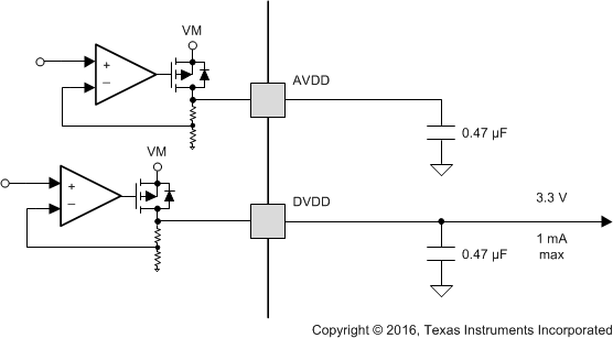
DRV8884 LDO_V_reg_lvsd39.gifFigure 22. LDO Diagram

If a digital input needs to be tied permanently high (that is, Mx, DECAY, or TRQ), it is preferable to tie the input to DVDD instead of an external regulator. This saves power when VM is not applied or in sleep mode; DVDD is disabled and current will not be flowing through the input pulldown resistors. For reference, logic level inputs have a typical pulldown of 100 kΩ, and tri-level inputs have a typical pulldown of 60 kΩ.