SLVSD39D October   2015  – March 2020 DRV8885

PRODUCTION DATA.  

  1. Features
  2. Applications
  3. Description
    1.     Device Images
      1.      Simplified Schematic
      2.      Microstepping Current Waveform
  4. Revision History
  5. Pin Configuration and Functions
    1.     Pin Functions
  6. Specifications
    1. 6.1 Absolute Maximum Ratings
    2. 6.2 ESD Ratings
    3. 6.3 Recommended Operating Conditions
    4. 6.4 Thermal Information
    5. 6.5 Electrical Characteristics
    6. 6.6 Indexer Timing Requirements
    7. 6.7 Typical Characteristics
  7. Detailed Description
    1. 7.1 Overview
    2. 7.2 Functional Block Diagram
    3. 7.3 Feature Description
      1. 7.3.1  Stepper Motor Driver Current Ratings
        1. 7.3.1.1 Peak Current Rating
        2. 7.3.1.2 RMS Current Rating
        3. 7.3.1.3 Full-Scale Current Rating
      2. 7.3.2  PWM Motor Drivers
      3. 7.3.3  Microstepping Indexer
      4. 7.3.4  Current Regulation
      5. 7.3.5  Controlling RREF With an MCU
        1. 7.3.5.1 Various Sources of Error
          1. 7.3.5.1.1 VRREF, ARREF, and RREF Error
          2. 7.3.5.1.2 VDAC Error
        2. 7.3.5.2 Application-Specific Error Calculations
      6. 7.3.6  Decay Modes
        1. 7.3.6.1 Mode 1: Slow Decay for Increasing and Decreasing Current
        2. 7.3.6.2 Mode 2: Slow Decay for Increasing Current, Mixed Decay for Decreasing Current
        3. 7.3.6.3 Mode 3: Mixed Decay for Increasing and Decreasing Current
      7. 7.3.7  Blanking Time
      8. 7.3.8  Charge Pump
      9. 7.3.9  LDO Voltage Regulator
      10. 7.3.10 Logic and Multi-Level Pin Diagrams
      11. 7.3.11 Protection Circuits
        1. 7.3.11.1 VM Undervoltage Lockout (UVLO)
        2. 7.3.11.2 VCP Undervoltage Lockout (CPUV)
        3. 7.3.11.3 Overcurrent Protection (OCP)
        4. 7.3.11.4 Thermal Shutdown (TSD)
    4. 7.4 Device Functional Modes
  8. Application and Implementation
    1. 8.1 Application Information
    2. 8.2 Typical Application
      1. 8.2.1 Design Requirements
      2. 8.2.2 Detailed Design Procedure
        1. 8.2.2.1 Stepper Motor Speed
        2. 8.2.2.2 Current Regulation
        3. 8.2.2.3 Decay Modes
      3. 8.2.3 Application Curves
  9. Power Supply Recommendations
    1. 9.1 Bulk Capacitance
  10. 10Layout
    1. 10.1 Layout Guidelines
    2. 10.2 Layout Example
  11. 11Device and Documentation Support
    1. 11.1 Documentation Support
      1. 11.1.1 Related Documentation
    2. 11.2 Receiving Notification of Documentation Updates
    3. 11.3 Community Resources
    4. 11.4 Trademarks
    5. 11.5 Electrostatic Discharge Caution
    6. 11.6 Glossary
  12. 12Mechanical, Packaging, and Orderable Information

Package Options

Mechanical Data (Package|Pins)
Thermal pad, mechanical data (Package|Pins)
Orderable Information

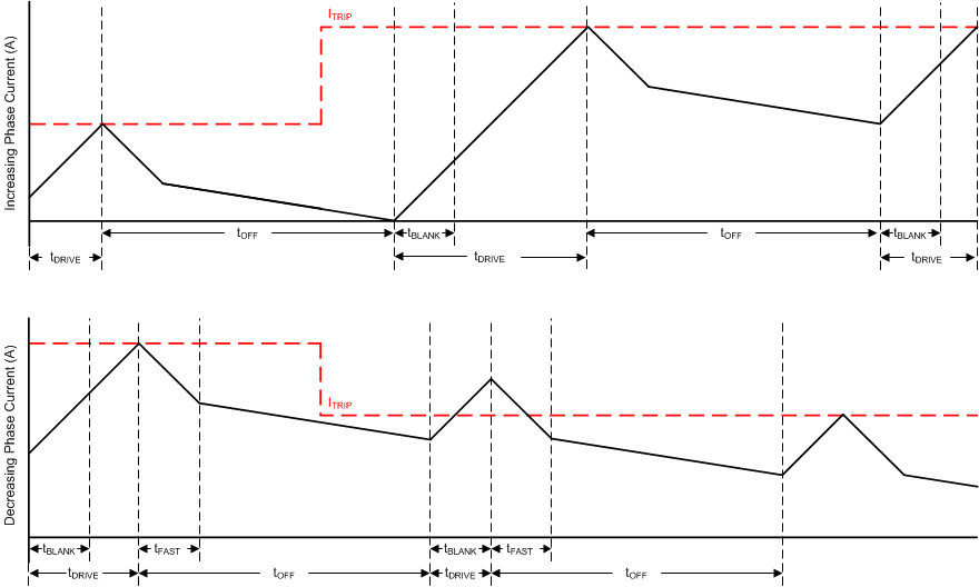
Mode 3: Mixed Decay for Increasing and Decreasing Current

DRV8885 mode_3_lvsd39.gifFigure 20. Mixed/Mixed Decay Mode

Mixed decay begins as fast decay for a time, followed by slow decay for the remainder of tOFF. In this mode, mixed decay occurs for both increasing and decreasing current steps.

This mode exhibits ripple larger than slow decay, but smaller than fast decay. On decreasing current steps, mixed decay will settle to the new ITRIP level faster than slow decay.

In cases where current is held for a long time (no input in the STEP pin) or at very low stepping speeds, slow decay may not properly regulate current because no back-EMF is present across the motor windings. In this state, motor current can rise very quickly, and requires an excessively large off-time. Increasing/decreasing mixed decay mode allows the current level to stay in regulation when no back-EMF is present across the motor windings.