SLVSDO1C January 2017 – March 2020 DRV8886AT
PRODUCTION DATA.
- 1 Features
- 2 Applications
- 3 Description
- 4 Revision History
- 5 Pin Configuration and Functions
- 6 Specifications
-
7 Detailed Description
- 7.1 Overview
- 7.2 Functional Block Diagram
- 7.3
Feature Description
- 7.3.1 Stepper Motor Driver Current Ratings
- 7.3.2 PWM Motor Drivers
- 7.3.3 Microstepping Indexer
- 7.3.4 Current Regulation
- 7.3.5 Controlling RREF With an MCU DAC
- 7.3.6 Decay Modes
- 7.3.7 Blanking Time
- 7.3.8 Charge Pump
- 7.3.9 Linear Voltage Regulators
- 7.3.10 Logic and Multi-Level Pin Diagrams
- 7.3.11 Protection Circuits
- 7.4 Device Functional Modes
- 8 Application and Implementation
- 9 Power Supply Recommendations
- 10Layout
- 11Device and Documentation Support
- 12Mechanical, Packaging, and Orderable Information
Package Options
Mechanical Data (Package|Pins)
Thermal pad, mechanical data (Package|Pins)
Orderable Information
7.3.6 Decay Modes
The DRV8886AT decay mode is selected by setting the quad-level DECAY pin to the voltage range listed in Table 21. The decay mode setting is latched on device enable.
Table 21. Decay Mode Settings
| DECAY | INCREASING STEPS | DECREASING STEPS |
|---|---|---|
| 100 mV
Can be tied to ground |
Slow decay | Mixed decay: 30% fast |
| 300 mV, 15 kΩ to GND | Mixed decay: 30% fast | Mixed decay: 30% fast |
| 1.0 V, 45 kΩ to GND | smart tune Ripple Control | smart tune Ripple Control |
| 2.9 V
Can be tied to DVDD |
smart tune Dynamic Decay | smart tune Dynamic Decay |
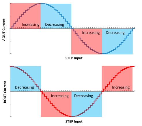
Figure 17 defines increasing and decreasing current. For the slow-mixed decay mode, the decay mode is set as slow during increasing current steps and mixed decay during decreasing current steps. In full step mode the decreasing steps decay mode is always used. In noncircular 1/2-step mode the increasing step decay mode is used after a level transition (0% to 100% and 0% to –100%). When the level transition is to a similar level (100% to 100% and –100% to –100%), the decreasing step decay mode is used.
 Figure 17. Definition of Increasing and Decreasing Steps