SLVSEC9C September 2019 – February 2020 DRV8904-Q1 , DRV8906-Q1 , DRV8908-Q1 , DRV8910-Q1 , DRV8912-Q1
PRODUCTION DATA.
- 1 Features
- 2 Applications
- 3 Description
- 4 Revision History
- 5 Device Comparison Table
- 6 Pin Configuration and Functions
- 7 Specifications
-
8 Detailed Description
- 8.1 Overview
- 8.2 Functional Block Diagram
- 8.3
Feature Description
- 8.3.1
Half Bridge Drivers
- 8.3.1.1
Control Modes
- 8.3.1.1.1 Continuous Mode (Without PWM)
- 8.3.1.1.2 Chopping Mode (With PWM)
- 8.3.1.1.3 Parallel Mode (Continuous Operation)
- 8.3.1.1.4
Parallel Mode (PWM Operation)
- 8.3.1.1.4.1 PWM Configuration
- 8.3.1.1.4.2 Free-Wheeling Mode (Synchronous Rectification) Disable / Enable
- 8.3.1.1.4.3 PWM Channels Mapping
- 8.3.1.1.4.4 PWM Channels Configuration (PWM Frequency and PWM Duty)
- 8.3.1.1.4.5 PWM Generators Disable
- 8.3.1.1.4.6 Half-Bridge Enable
- 8.3.1.1.4.7 PWM Generators Enable
- 8.3.1.2 Half-Bridge Drive Architecture
- 8.3.1.1
Control Modes
- 8.3.2 Pin Diagrams
- 8.3.3 Protection Circuits
- 8.3.1
Half Bridge Drivers
- 8.4 Device Functional Modes
- 8.5 Programming
- 8.6
Register Map
- 8.6.1
DRV8912-Q1 and DRV8910-Q1 Register Maps
- 8.6.1.1
Status Registers
- 8.6.1.1.1 IC Status (IC_STAT) Register (Address = 0x00) [reset = 0x00]
- 8.6.1.1.2 Overcurrent Protection (OCP) Status 1 (OCP_STAT_1) Register (Address = 0x01) [reset = 0x00]
- 8.6.1.1.3 Overcurrent Protection (OCP) Status 2 (OCP_STAT_2) Register (Address = 0x02) [reset = 0x00]
- 8.6.1.1.4 Overcurrent Protection (OCP) Status 3 (OCP_STAT_3) Register (Address = 0x03) [reset = 0x00]
- 8.6.1.1.5 Open-Load Detect (OLD) Status 1 (OLD_STAT_1) Register (Address = 0x04) [reset = 0x00]
- 8.6.1.1.6 Open-Load Detect (OLD) Status 2 (OLD_STAT_2) Register (Address = 0x05) [reset = 0x00]
- 8.6.1.1.7 Open-Load Detect (OLD) Status 3 (OLD_STAT_3) Register (Address = 0x06) [reset = 0x00]
- 8.6.1.2
Control Registers
- 8.6.1.2.1 Configuration (CONFIG_CTRL) Register (Address = 0x07) [reset = 0x00]
- 8.6.1.2.2 Operation Control 1 (OP_CTRL_1) Register (Address = 0x08) [reset = 0x00]
- 8.6.1.2.3 Operation Control 2 (OP_CTRL_2) Register (Address = 0x09) [reset = 0x00]
- 8.6.1.2.4 Operation Control 3 (OP_CTRL_3) Register (Address = 0x0A) [reset = 0x00]
- 8.6.1.2.5 PWM Control 1 (PWM_CTRL_1) Register (Address = 0x0B) [reset = 0x00]
- 8.6.1.2.6 PWM Control 2 (PWM_CTRL_2) Register (Address = 0x0C) [reset = 0x00]
- 8.6.1.2.7 Free-Wheeling Control 1 (FW_CTRL_1) Register (Address = 0x0D) [reset = 0x00]
- 8.6.1.2.8 Free-Wheeling Control 2 (FW_CTRL_2) Register (Address = 0x0E) [reset = 0x00]
- 8.6.1.2.9 PWM Map Control 1 (PWM_MAP_CTRL_1) Register (Address = 0x0F) [reset = 0x00]
- 8.6.1.2.10 PWM Map Control 2 (PWM_MAP_CTRL_2) Register (Address = 0x10) [reset = 0x00]
- 8.6.1.2.11 PWM Map Control 3 (PWM_MAP_CTRL_3) Register (Address = 0x11) [reset = 0x00]
- 8.6.1.2.12 PWM Frequency Control (PWM_FREQ_CTRL) Register (Address = 0x12) [reset = 0x00]
- 8.6.1.2.13 PWM Duty Control Channel 1 (PWM_DUTY_CH1) Register (Address = 0x13) [reset = 0x00]
- 8.6.1.2.14 PWM Duty Control Channel 2 (PWM_DUTY_CH2) Register (Address = 0x14) [reset = 0x00]
- 8.6.1.2.15 PWM Duty Control Channel 3 (PWM_DUTY_CH3) Register (Address = 0x15) [reset = 0x00]
- 8.6.1.2.16 PWM Duty Control Channel 4 (PWM_DUTY_CH4) Register (Address = 0x16) [reset = 0x00]
- 8.6.1.2.17 Slew Rate Control 1 (SR_CTRL_1) Register (Address = 0x17) [reset = 0x00]
- 8.6.1.2.18 Slew Rate Control 2 (SR_CTRL_2) Register (Address = 0x18) [reset = 0x00]
- 8.6.1.2.19 Open-Load Detect (OLD) Control 1 (OLD_CTRL_1) Register (Address = 0x19) [reset = 0x00]
- 8.6.1.2.20 Open-Load Detect (OLD) Control 2 (OLD_CTRL_2) Register (Address = 0x1A) [reset = 0x00]
- 8.6.1.2.21 Open-Load Detect (OLD) Control 3 (OLD_CTRL_3) Register (Address = 0x1B) [reset = 0x00]
- 8.6.1.2.22 Open-Load Detect (OLD) Control 4 (OLD_CTRL_4) Register (Address = 0x24) [reset = 0x00]
- 8.6.1.1
Status Registers
- 8.6.2
DRV8908-Q1, DRV8906-Q1 and DRV8904-Q1 Register Maps
- 8.6.2.1
Status Registers
- 8.6.2.1.1 IC Status (IC_STAT) Register (Address = 0x00) [reset = 0x00]
- 8.6.2.1.2 Overcurrent Protection (OCP) Status 1 (OCP_STAT_1) Register (Address = 0x01) [reset = 0x00]
- 8.6.2.1.3 Overcurrent Protection (OCP) Status 2 (OCP_STAT_2) Register (Address = 0x02) [reset = 0x00]
- 8.6.2.1.4 Overcurrent Protection (OCP) Status 3 (OCP_STAT_3) Register (Address = 0x03) [reset = 0x00]
- 8.6.2.1.5 Open-Load Detect (OLD) Status 1 (OLD_STAT_1) Register (Address = 0x04) [reset = 0x00]
- 8.6.2.1.6 Open-Load Detect (OLD) Status 2 (OLD_STAT_2) Register (Address = 0x05) [reset = 0x00]
- 8.6.2.1.7 Open-Load Detect (OLD) Status 3 (OLD_STAT_3) Register (Address = 0x06) [reset = 0x00]
- 8.6.2.2
Control Registers
- 8.6.2.2.1 Configuration (CONFIG_CTRL) Register (Address = 0x07) [reset = 0x00]
- 8.6.2.2.2 Operation Control 1 (OP_CTRL_1) Register (Address = 0x08) [reset = 0x00]
- 8.6.2.2.3 Operation Control 2 (OP_CTRL_2) Register (Address = 0x09) [reset = 0x00]
- 8.6.2.2.4 Operation Control 3 (OP_CTRL_3) Register (Address = 0x0A) [reset = 0x00]
- 8.6.2.2.5 PWM Control 1 (PWM_CTRL_1) Register (Address = 0x0B) [reset = 0x00]
- 8.6.2.2.6 PWM Control 2 (PWM_CTRL_2) Register (Address = 0x0C) [reset = 0x00]
- 8.6.2.2.7 Free-Wheeling Control 1 (FW_CTRL_1) Register (Address = 0x0D) [reset = 0x00]
- 8.6.2.2.8 Free-Wheeling Control 2 (FW_CTRL_2) Register (Address = 0x0E) [reset = 0x00]
- 8.6.2.2.9 PWM Map Control 1 (PWM_MAP_CTRL_1) Register (Address = 0x0F) [reset = 0x00]
- 8.6.2.2.10 PWM Map Control 2 (PWM_MAP_CTRL_2) Register (Address = 0x10) [reset = 0x00]
- 8.6.2.2.11 PWM Map Control 3 (PWM_MAP_CTRL_3) Register (Address = 0x11) [reset = 0x00]
- 8.6.2.2.12 PWM Map Control 4 (PWM_MAP_CTRL_4) Register (Address = 0x12) [reset = 0x00]
- 8.6.2.2.13 PWM Frequency Control 1 (PWM_FREQ_CTRL_1) Register (Address = 0x13 [reset = 0x00]
- 8.6.2.2.14 PWM Frequency Control 2 (PWM_FREQ_CTRL_2) Register (Address = 0x14 [reset = 0x00]
- 8.6.2.2.15 PWM Duty Control Channel 1 (PWM_DUTY_CH1) Register (Address = 0x15) [reset = 0x00]
- 8.6.2.2.16 PWM Duty Control Channel 2 (PWM_DUTY_CH2) Register (Address = 0x16) [reset = 0x00]
- 8.6.2.2.17 PWM Duty Control Channel 3 (PWM_DUTY_CH3) Register (Address = 0x17) [reset = 0x00]
- 8.6.2.2.18 PWM Duty Control Channel 4 (PWM_DUTY_CH4) Register (Address = 0x18) [reset = 0x00]
- 8.6.2.2.19 PWM Duty Control Channel 5 (PWM_DUTY_CH5) Register (Address = 0x19) [reset = 0x00]
- 8.6.2.2.20 PWM Duty Control Channel 6 (PWM_DUTY_CH6) Register (Address = 0x1A) [reset = 0x00]
- 8.6.2.2.21 PWM Duty Control Channel 7 (PWM_DUTY_CH7) Register (Address = 0x1B) [reset = 0x00]
- 8.6.2.2.22 PWM Duty Control Channel 8 (PWM_DUTY_CH8) Register (Address = 0x1C) [reset = 0x00]
- 8.6.2.2.23 Slew Rate Control 1 (SR_CTRL_1) Register (Address = 0x1D [reset = 0x00]
- 8.6.2.2.24 Slew Rate Control 2 (SR_CTRL_2) Register (Address = 0x1E) [reset = 0x00]
- 8.6.2.2.25 Open-Load Detect (OLD) Control 1 (OLD_CTRL_1) Register (Address = 0x1F) [reset = 0x00]
- 8.6.2.2.26 Open-Load Detect (OLD) Control 2 (OLD_CTRL_2) Register (Address = 0x20) [reset = 0x00]
- 8.6.2.2.27 Open-Load Detect (OLD) Control 3 (OLD_CTRL_3) Register (Address = 0x21) [reset = 0x00]
- 8.6.2.2.28 Open Load Detect (OLD) Control 4 (OLD_CTRL_4) Register (Address = 0x22) [reset = 0x00]
- 8.6.2.2.29 Open Load Detect (OLD) Control 5 (OLD_CTRL_5) Register (Address = 0x23) [reset = 0x00]
- 8.6.2.2.30 Open Load Detect (OLD) Control 6 (OLD_CTRL_6) Register (Address = 0x24) [reset = 0x00]
- 8.6.2.1
Status Registers
- 8.6.1
DRV8912-Q1 and DRV8910-Q1 Register Maps
- 9 Application and Implementation
- 10Power Supply Recommendations
- 11Layout
- 12Device and Documentation Support
- 13Mechanical, Packaging, and Orderable Information
Package Options
Mechanical Data (Package|Pins)
- PWP|24
Thermal pad, mechanical data (Package|Pins)
- PWP|24
Orderable Information
8.3.3.5.2 Low-current OLD
Low-current open-load detection is another type of active open-load detection in the DRV89XX-Q1 devices. In low-current open-load detection, the current detection threshold is around 10x lower than the active open-load detection scheme. This feature gives the user flexibility to detect a valid open-load condition when driving loads that require low current.
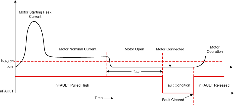
As shown in Figure 64, if the low-side MOSFET is in operating condition (switched-ON) and the current flowing in the particular MOSFET is lower than the low-current active open-load current threshold (IOLD_LOW) for at least open-load detection deglitch time (tOLD), then an open-load condition is detected. The OLD bit in the IC status (IC_STAT) register is set, the HBX_LS_OLD bit in the open-load status register (OLD_STAT_X) is set and nFAULT pin is driven low during an open-load detect. Normal operation resumes (driver operation and the nFAULT pin is released) when the open-load condition is removed and CLR_FLT command is issued. The OLD bit remains set until cleared through the CLR_FLT bit.
 Figure 64. Low-Current OLD
 NOTE
The low-current OLD has following limitations
- This feature is only applicable for the current flowing in low-side FET.
- Once this mode is enabled the corresponding over-current threshold for the low-side FET is also reduced by 11 times (~120 mA min.).
- The RDS(on) of the low side FET will increase by 11 times (~7.5 Ω typical), hence the thermal performance has to be monitored. However, for the lower current the thermal dissipation is limited.
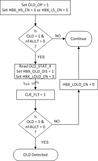
Figure 65 shows the flowchart for implementing the low-current active OLD in continuous mode of operation. Following are the steps to configure and detect the low-current active OLD in the DRV89XX-Q1 device.
- Enable OLD by setting the OLD_OP bit in OLD_CTRL_2 register. This setting will ensure that the OUTX outputs continue to operate when and OLD fault occurs.
- Enable the full-bridge operation by setting the individual HBX_HS_EN/HBX_LS_EN bits in operation control (OP_CTRL_1, OP_CTRL_2 and OP_CTRL_3) registers.
- Check for the nFAULT pin status and the OLD fault in the IC_STAT register.
- If the nFAULT pin is low and the OLD fault is high, then check for the individual HBX_HS_OLD/HBX_LS_OLD bits in OLD status (OLD_STAT_1, OLD_STAT_2 and OLD_STAT_3) registers.
- Disable OLD using the HBX_OLD_DIS bits for the OUTX pins acting as high-side drivers.
- Enable the low-current OLD mode for the half-bridge which low-side is operating by using the HBX_LOLD_EN bit in OLD control (OLD_CTRL_3 and OLD_CTRL_4) registers. This will also disable the high-side OLD for the particular half-bridge.
- Wait for the open-load deglitch time (tOLD).
- Issue the clear fault command (CLR_FLT) to release the nFAULT pin and clear the OLD bits if low-current OLD is not detected.
- If the OLD bit is high and the nFAULT pin is not released (low), then low-current OLD fault is detected.
NOTE
The low-current OLD is applicable only for low-side FETs. The user has to enable the low-current OLD mode for the corresponding low-side FET.
 Figure 65. Flowchart for Enabling Low-Current OLD (Continuous Mode)