SNOSC82B August 2012 – June 2015 DS1776QML
PRODUCTION DATA.
- 1Features
- 2Description
- 3Revision History
- 4Pin Configuration and Functions
-
5Specifications
- 5.1 Absolute Maximum Ratings
- 5.2 ESD Ratings
- 5.3 Recommend Operating Conditions
- 5.4 Thermal Information
- 5.5 Quality Conformance Inspection
- 5.6 Pi Bus Transceiver DS1776 DC Parameters
- 5.7 Pi Bus Transceiver DS1776 AC Parameters: B To A Path
- 5.8 Pi Bus Transceiver DS1776 AC Parameters: A To B Path
- 5.9 Pi Bus Transceiver DS1776 AC Parameters: Setup / Hold / Pulse Width Specifications
- 5.10 Test Circuit And Waveforms
- 6Detailed Description
- 7Device and Documentation Support
- 8Mechanical, Packaging, and Orderable Information
Package Options
Mechanical Data (Package|Pins)
- FK|28
Thermal pad, mechanical data (Package|Pins)
Orderable Information
1 Features
- Similar to BTL
- Low Power ICCL = 41 mA max
- B Output Controlled Ramp Rate
- B input Noise Immunity, Typically 4 ns
- Pin and Function Compatible with Signetics 54F776
2 Description
The DS1776 is an octal PI-bus Transceiver. The A to B path is latched. B outputs are open collector with series Schottky diode, ensuring minimum B output loading. B outputs also have ramped rise and fall times (2.5 ns typical), ensuring minimum PI-bus ringing. B inputs have glitch rejection circuitry, 4 ns typical.
Designed using Texas Instruments's Bi-CMOS process for both low operating and disabled power. AC performance is optimized for the PI-Bus inter-operability requirements.
The DS1776 is an octal latched transceiver and is intended to provide the electrical interface to a high performance wired-or bus. This bus has a loaded characteristic impedance range of 20Ω to 50Ω and is terminated on each end with a 30Ω to 40Ω resistor.
The DS1776 is an octal bidirectional transceiver with open collector B and TRI-STATE A port output drivers. A latch function is provided for the A port signals. The B port output driver is designed to sink 100 mA from 2V and features a controlled linear ramp to minimize crosstalk and ringing on the bus.
A separate high level control voltage (VX) is provided to prevent the A side output high level from exceeding future high density processor supply voltage levels. For 5V systems, VX is tied to VCC.
Device Information(1)
| PART NUMBER | PACKAGE | BODY SIZE (NOM) |
|---|---|---|
| DS1776QML | LCCC (FK) | 11.43 mm x 11.43 mm |
- For all available packages, see the orderable addendum at the end of the datasheet.
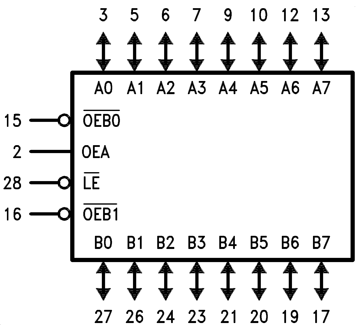
Logic Symbol

3 Revision History
Changes from A Revision (April 2013) to B Revision
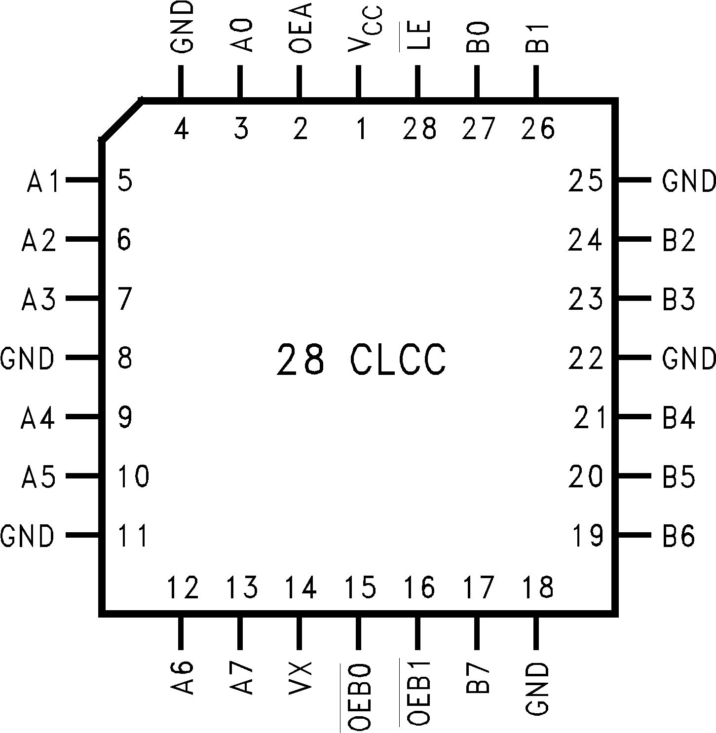
4 Pin Configuration and Functions

Pin Descriptions
| PIN | I/O | DESCRIPTION | |
|---|---|---|---|
| NAME | NO. | ||
| A0 | 3 | I/O | TTL Level, latched input/TRI-STATE output (with VX control option) |
| A1 | 5 | I/O | |
| A2 | 6 | I/O | |
| A3 | 7 | I/O | |
| A4 | 9 | I/O | |
| A5 | 10 | I/O | |
| A6 | 12 | I/O | |
| A7 | 13 | I/O | |
| B0 | 27 | I/O | Data input with special threshold circuitry to reject noise/Open Collector output, High current drive |
| B1 | 26 | I/O | |
| B2 | 24 | I/O | |
| B3 | 23 | I/O | |
| B4 | 21 | I/O | |
| B5 | 20 | I/O | |
| B6 | 19 | I/O | |
| B7 | 17 | I/O | |
| OEB 0 | 15 | I | Enables the B outputs when both pins are low |
| OEB 1 | 16 | I | |
| OEA | 2 | I | Enables the A outputs when High |
| LE | 28 | I | Latched when High (a special delay feature is built in for proper enabling times) |
| VX | 14 | I | Clamping voltage keeping VOH from rising above VX (VX = VCC for normal use) |