SNLS243H September 2006 – March 2016 DS25MB100
PRODUCTION DATA.
- 1 Features
- 2 Applications
- 3 Description
- 4 Revision History
- 5 Pin Configuration and Functions
- 6 Specifications
- 7 Parameter Measurement Information
- 8 Detailed Description
- 9 Application and Implementation
- 10Power Supply Recommendations
- 11Layout
- 12Device and Documentation Support
- 13Mechanical, Packaging, and Orderable Information
Package Options
Mechanical Data (Package|Pins)
- NJK|36
Thermal pad, mechanical data (Package|Pins)
Orderable Information
1 Features
- 2:1 Multiplexer and 1:2 Buffer
- 0.25-Gbps to 2.5-Gbps Fully Differential Data Paths
- Fixed Input Equalization
- Programmable Output Pre-Emphasis
- Independent Pre-Emphasis Controls
- Programmable Loopback Modes
- On-Chip Terminations
- ESD Rating of 6-kV HBM
- 3.3-V Supply
- Low power, 0.45 W Typical
- Lead-Less WQFN-36 Package
- −40°C to +85°C Operating Temperature Range
2 Applications
- Backplane Drivers or Cable Driver
- Redundancy and Signal Conditioning Applications
- CPRI/OBSAI
3 Description
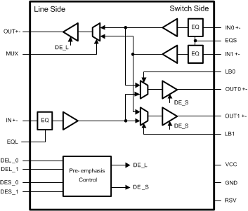
The DS25MB100 device is a signal conditioning 2:1 multiplexer and 1:2 fan-out buffer designed for use in backplane-redundancy or cable driving applications. Signal conditioning features include continuous time linear equalization (CTLE) and programmable output pre-emphasis that enable data communication in FR4 backplane up to 2.5 Gbps. Each input stage has a fixed equalizer to reduce ISI distortion from board traces.
All output drivers have four selectable levels of pre-emphasis to compensate for transmission losses from long FR4 backplane or cable attenuation reducing deterministic jitter. The pre-emphasis levels can be independently controlled for the line-side and switch-side drivers. The internal loopback paths from switch-side input to switch-side output enable at-speed system testing. All receiver inputs are internally terminated with 100-Ω differential terminating resistors. All driver outputs are internally terminated with 50-Ω terminating resistors to VCC.
Device Information(1)
| PART NUMBER | PACKAGE | BODY SIZE (NOM) |
|---|---|---|
| DS25MB100 | WQFN (36) | 6.00 mm × 6.00 mm |
- For all available packages, see the orderable addendum at the end of the data sheet.
Simplified Block Diagram
