SNLS542C October 2016 – December 2020 DS280MB810
PRODUCTION DATA
- 1 Features
- 2 Applications
- 3 Description
- 4 Revision History
- 5 Description (continued)
- 6 Pin Configuration and Functions
- 7 Specifications
- 8 Detailed Description
- 9 Application and Implementation
- 10Power Supply Recommendations
- 11Layout
- 12Device and Documentation Support
- 13Mechanical, Packaging, and Orderable Information
Package Options
Mechanical Data (Package|Pins)
- ZBL|135
Thermal pad, mechanical data (Package|Pins)
Orderable Information
9.2.2 Front-Port Applications
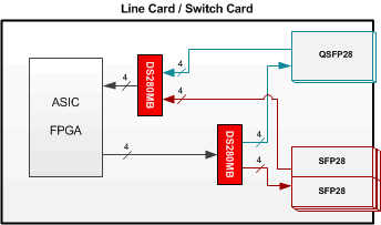
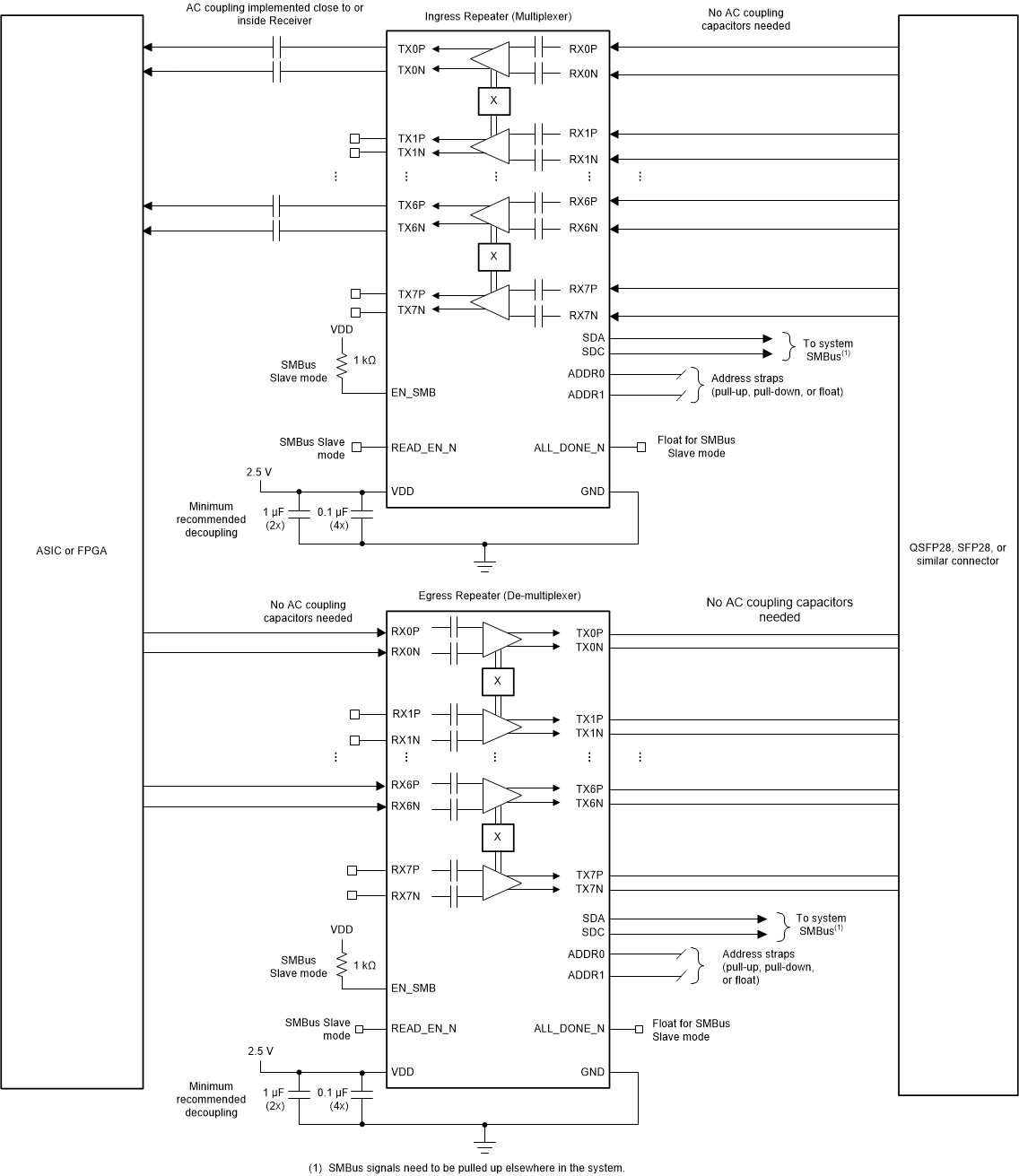
The DS280MB810 has strong equalization capabilities that allow it to equalize insertion loss and extend the reach of front-port channels by 17 dB beyond the normal capabilities of the ASIC while supporting CAUI-4 and CR4 electrical requirements. The DS280MB810 is designed to apply gain in a linear fashion in order to support longer distances between the switch ASIC and the front-port module. Figure 9-5 illustrates a configuration where two DS280MB810s are used to mux between one QSFP28 port and four SFP28 ports. Figure 9-9 shows the simplified schematic for this application.
 Figure 9-5 Front-port application block diagram
Standard front-port modules have AC coupling capacitors included inside the module. The DS280MB810, therefore, is ideal for front-port Egress signal conditioning applications since it includes AC coupling capacitors on the input (RX) side and does not include AC coupling capacitors on the output (TX) side.
 Figure 9-6 DS280MB810 recommended for front-port Egress
The optimum solution for front-port Ingress signal conditioning applications depends on whether the ASIC RX supports DC coupling and whether it can support an input common mode voltage of 1.05 V. For further guidance on determining if the ASIC RX supports DC coupling, refer to Figure 9-2. If the ASIC RX supports DC coupling and can tolerate an input common mode voltage of 1.05-V or less, then the DS280MB810 is the optimum solution for front-port Ingress signal conditioning. If the ASIC RX does not support DC coupling or cannot tolerate an input common mode voltage of 1.05-V, then the pin-compatible DS280DF810 Retimer with cross-point, which has integrated AC Coupling capacitors on both RX and TX, may be the optimum solution.
 Figure 9-7 DS280MB810 recommended for front-port Ingress
 Figure 9-8 DS280MB810 or DS280DF810 recommended for front-port Ingress
 Figure 9-9 Front-port application simplified schematic