SNLS542C October   2016  – December 2020 DS280MB810

PRODUCTION DATA  

  1. Features
  2. Applications
  3. Description
  4. Revision History
  5. Description (continued)
  6. Pin Configuration and Functions
  7. Specifications
    1. 7.1 Absolute Maximum Ratings
    2. 7.2 ESD Ratings
    3. 7.3 Recommended Operating Conditions
    4. 7.4 Thermal Information
    5. 7.5 Electrical Characteristics
    6. 7.6 Timing Requirements – Serial Management Bus Interface
    7. 7.7 Typical Characteristics
  8. Detailed Description
    1. 8.1 Overview
    2. 8.2 Functional Block Diagram
    3. 8.3 Feature Description
      1. 8.3.1 Device Data Path Operation
      2. 8.3.2 AC-coupled Receiver Inputs
      3. 8.3.3 Signal Detect
      4. 8.3.4 2-Stage CTLE
      5. 8.3.5 Driver DC Gain Control
      6. 8.3.6 2x2 Cross-point Switch
      7. 8.3.7 Configurable SMBus Address
    4. 8.4 Device Functional Modes
      1. 8.4.1 SMBus Slave Mode Configuration
      2. 8.4.2 SMBus Master Mode Configuration (EEPROM Self Load)
    5. 8.5 Programming
      1. 8.5.1 Transfer of Data with the SMBus Interface
    6. 8.6 Register Maps
      1. 8.6.1 Register Types: Global, Shared, and Channel
      2. 8.6.2 Global Registers: Channel Selection and ID Information
      3. 8.6.3 Shared Registers
      4. 8.6.4 Channel Registers
  9. Application and Implementation
    1. 9.1 Application Information
    2. 9.2 Typical Application
      1. 9.2.1 Backplane and Mid-Plane Reach Extension
        1. 9.2.1.1 Design Requirements
        2. 9.2.1.2 Detailed Design Procedure
      2. 9.2.2 Front-Port Applications
        1. 9.2.2.1 Design Requirements
        2. 9.2.2.2 Detailed Design Procedure
      3. 9.2.3 Application Curves
        1. 9.2.3.1 Pattern Generator Characteristics
        2. 9.2.3.2 Equalizing Moderate Pre-Channel Loss
        3. 9.2.3.3 Equalizing High Pre-Channel Loss
        4. 9.2.3.4 Equalizing High Pre-Channel Loss and Moderate Post-Channel Loss
    3. 9.3 Initialization Set Up
  10. 10Power Supply Recommendations
  11. 11Layout
    1. 11.1 Layout Guidelines
    2. 11.2 Layout Examples
      1. 11.2.1 Stripline Example
      2. 11.2.2 Microstrip Example
  12. 12Device and Documentation Support
    1. 12.1 Documentation Support
      1. 12.1.1 Related Documentation
    2. 12.2 Receiving Notification of Documentation Updates
    3. 12.3 Support Resources
    4. 12.4 Trademarks
  13. 13Mechanical, Packaging, and Orderable Information

Package Options

Mechanical Data (Package|Pins)
Thermal pad, mechanical data (Package|Pins)
Orderable Information

Backplane and Mid-Plane Reach Extension

The DS280MB810 has strong equalization capabilities that allow it to equalize insertion loss and extend the reach of backplane channels by 17+ dB beyond the normal capabilities of the ASICs operating over the channel. The DS280MB810 is designed to apply gain in a linear fashion. Whenever system design constraints allow, the DS280MB810 should be placed with the higher loss channel segment at the input and the lower loss channel segment at the output; however, since the DS280MB810 operates in a linear fashion, it can also be used in applications where the lower loss channel segment is at the input and the higher loss channel segment is at the output. Figure 9-3 shows a typical backplane and mid-plane configuration using the DS280MB810 to perform equalization and signal distribution for failover or redundancy. Figure 9-4 shows the corresponding simplified schematic for this application.
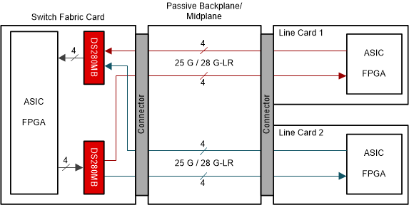
GUID-29DD0817-C9B9-4869-9557-4E8374119A13-low.gifFigure 9-3 Typical backplane and mid-plane application block diagram
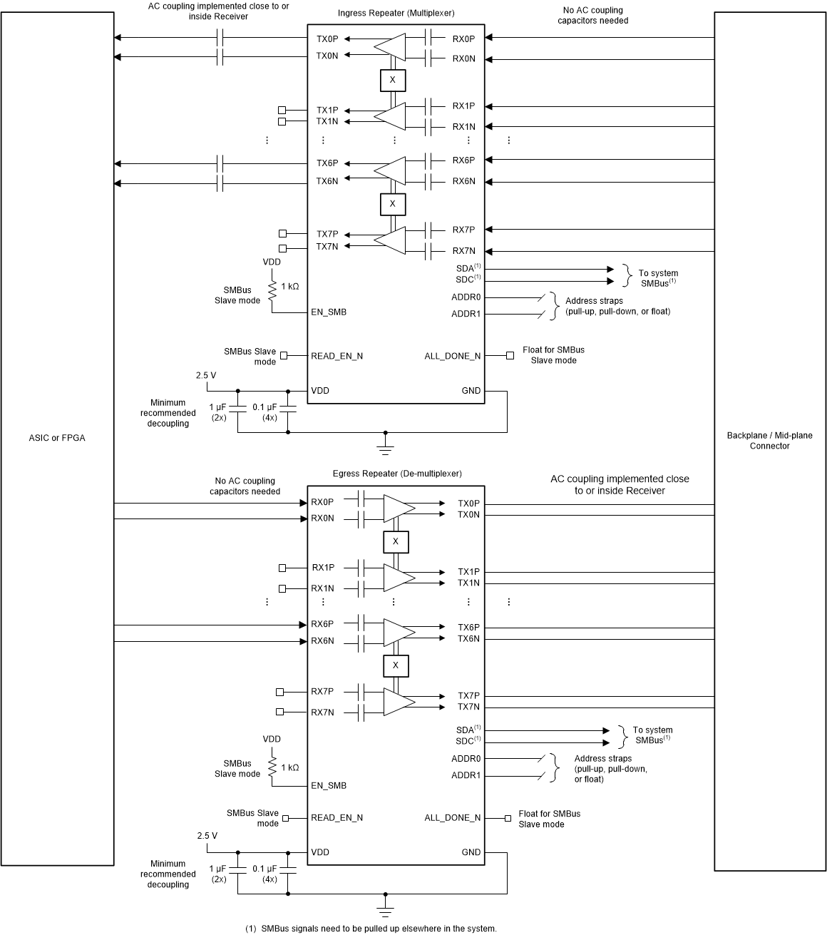
GUID-A4CC05C6-25C2-455D-B72D-BE97553BE73E-low.gifFigure 9-4 Typical backplane and mid-plane simplified schematic