SNLS672 August 2020 – MONTH DS90LV028A-Q1
PRODUCTION DATA
- 1 Features
- 2 Applications
- 3 Description
- 4 Revision History
- 5 Pin Configuration and Functions
- 6 Specifications
- 7 Parameter Measurement Information
- 8 Detailed Description
- 9 Application and Implementation
- 10Power Supply Recommendations
- 11Layout
- 12Device and Documentation Support
- 13Mechanical, Packaging, and Orderable Information
Package Options
Mechanical Data (Package|Pins)
- DQF|8
Thermal pad, mechanical data (Package|Pins)
Orderable Information
3 Description
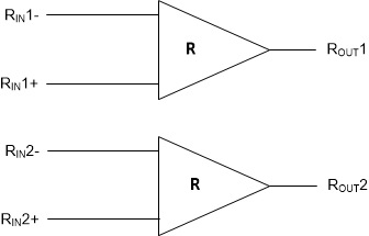
The DS90LV028A-Q1 is a dual CMOS differential line receiver designed for applications requiring ultra low power dissipation, low noise and high data rates. The device is designed to support data rates in excess of 400 Mbps (200 MHz) utilizing Low Voltage Differential Signaling (LVDS) technology.
The DS90LV028A-Q1 accepts low voltage (350 mV typical) differential input signals and translates them to 3 V CMOS output levels. The DS90LV028A-Q1 has a flow-through design for easy PCB layout.
The DS90LV028A-Q1 and companion LVDS line driver DS90LV027AQ provide a new alternative to high power PECL/ECL devices for high speed point-to-point interface applications.
| PART NUMBER | PACKAGE | BODY SIZE (NOM) |
|---|---|---|
| DS90LV028A-Q1 | WSON (DQF 8) | 2.00 mm x 2.00 mm |
 Functional Diagram