SNLS507C September   2016  – December 2022 DS90UB934-Q1

PRODUCTION DATA  

  1.   Features
  2. 1Applications
  3. 2Description
  4. 3Revision History
  5.   Pin Configuration and Functions
  6. 4Specifications
    1. 4.1 Absolute Maximum Ratings
    2. 4.2 ESD Ratings
    3. 4.3 Recommended Operating Conditions
    4. 4.4 Thermal Information
    5. 4.5 DC Electrical Characteristics
    6. 4.6 AC Electrical Characteristics
    7. 4.7 Recommended Timing for the Serial Control Bus
    8. 4.8 Typical Characteristics
  7. 5Detailed Description
    1. 5.1 Overview
      1. 5.1.1 Functional Description
    2. 5.2 Functional Block Diagram
    3. 5.3 Feature Description
      1. 5.3.1 Serial Frame Format
      2. 5.3.2 Line Rate Calculations for the DS90UB933/934
      3. 5.3.3 Deserializer Multiplexer Input
    4. 5.4 Device Functional Modes
      1. 5.4.1 RX MODE Pin
      2. 5.4.2 DVP Output Control
        1. 5.4.2.1 LOCK Status
      3. 5.4.3 Input Jitter Tolerance
      4. 5.4.4 Adaptive Equalizer
      5. 5.4.5 Channel Monitor Loop-Through Output Driver
        1. 5.4.5.1 Code Example for CMLOUT FPD3 RX Port 0:
      6. 5.4.6 GPIO Support
        1. 5.4.6.1 Back Channel GPIO
        2. 5.4.6.2 GPIO Pin Status
        3. 5.4.6.3 Other GPIO Pin Controls
        4. 5.4.6.4 FrameSync Operation
          1. 5.4.6.4.1 External FrameSync Control
          2. 5.4.6.4.2 Internally Generated FrameSync
            1. 5.4.6.4.2.1 Code Example for Internally Generated FrameSync
    5. 5.5 Programming
      1. 5.5.1 Serial Control Bus
        1. 5.5.1.1 I2C Target Operation
        2. 5.5.1.2 Remote Target Operation
        3. 5.5.1.3 Remote I2C Targets Data Throughput
        4. 5.5.1.4 Remote Target Addressing
        5. 5.5.1.5 Broadcast Write to Remote Target Devices
        6. 5.5.1.6 Code Example for Broadcast Write
      2. 5.5.2 Interrupt Support
        1. 5.5.2.1 Code Example to Enable Interrupts
        2. 5.5.2.2 FPD-Link III Receive Port Interrupts
        3. 5.5.2.3 Code Example to Readback Interrupts
        4. 5.5.2.4 Built-In Self Test (BIST)
          1. 5.5.2.4.1 BIST Configuration and Status
    6. 5.6 Register Maps
      1. 5.6.1 Register Description
      2. 5.6.2 Registers
      3. 5.6.3 Indirect Access Registers
      4. 5.6.4 Indirect Access Register Map
        1. 5.6.4.1 FPD3 Channel 0 Registers
        2. 5.6.4.2 FPD3 Channel 1 Registers
        3. 5.6.4.3 FPD3 RX Shared Registers
  8. 6Application and Implementation
    1. 6.1 Application Information
    2. 6.2 Power Over Coax
    3. 6.3 Typical Application
      1. 6.3.1 Design Requirements
      2. 6.3.2 Detailed Design Procedure
      3. 6.3.3 Application Curves
    4. 6.4 System Examples
    5. 6.5 Power Supply Recommendations
      1. 6.5.1 VDD Power Supply
      2. 6.5.2 Power-Up Sequencing
      3. 6.5.3 PDB Pin
      4. 6.5.4 Ground
    6. 6.6 Layout
      1. 6.6.1 Layout Guidelines
        1. 6.6.1.1 DVP Interface Guidelines
      2. 6.6.2 Layout Example
  9.   Mechanical, Packaging, and Orderable Information
  10. 7Device and Documentation Support
    1. 7.1 Documentation Support
      1. 7.1.1 Related Documentation
    2. 7.2 Glossary
    3. 7.3 Receiving Notification of Documentation Updates
    4. 7.4 Support Resources
    5. 7.5 Trademarks
  11.   Mechanical, Packaging, and Orderable Information

Package Options

Mechanical Data (Package|Pins)
Thermal pad, mechanical data (Package|Pins)
Orderable Information

Channel Monitor Loop-Through Output Driver

The DS90UB934-Q1 includes an internal channel monitor loop-through output on the CMLOUTP/N pins. A buffered loop-through output driver is provided on the CMLOUTP/N for observing jitter after equalization for each of the two RX receive channels. The CMLOUT monitors the post EQ stage, thus providing the recovered input of the deserializer signal. The measured serial data width on the CMLOUT loop-through is the total jitter including the internal driver, AEQ, back channel echo, etc. Each channel also has its own CMLOUT monitor and can be used for debug purposes. This CMLOUT is useful in identifying gross signal conditioning issues. The intrinsic jitter, JCML, represents the amount of jitter seen with a clean serial stream applied to the FPD-Link III input pins. When the total jitter is measured on CMLOUTP and CMLOUTN, the typical intrinsic jitter value can be subtracted to get an approximation of how much jitter is seen at the RIN[1:0]± input pins.

Table 5-6 includes details on selecting the corresponding RX receiver of CMLOUTP/N configuration.

Table 5-5 CML Monitor Output Driver
PARAMETERTEST CONDITIONSPINMINTYPMAXUNIT
JCMLCMLOUT Differential Output Intrinsic JitterClean clock fed into FPD-Link III input
RL = 100 Ω
(Figure 5-4)
CMLOUTP, CMLOUTN0.15UI(1)
UI – Unit interval is equivalent to one ideal serialized data bit width. The UI scales with serializer input PCLK frequency.
10-bit mode: 1 UI = 1 / ( PCLK_Freq. /2 x 28 )
12-bit HF mode: 1 UI = 1 / ( PCLK_Freq. x 2/3 x 28 )
12-bit LF mode: 1 UI = 1 / ( PCLK_Freq. x 28 )
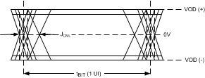
GUID-3CCF9EAA-FD6F-4391-87EB-FC1A85093242-low.gifFigure 5-4 CMLOUT Output Driver
Table 5-6 Channel Monitor Loop-Through Output Configuration
FPD3 RX Port 0FPD3 RX Port 1
ENABLE MAIN LOOPTHRU DRIVER0xB0 = 0x14
0xB1 = 0x00
0xB2 = 0x80
0xB0 = 0x14
0xB1 = 0x00
0xB2 = 0x80
SELECT CHANNEL MUX0xB1 = 0x02
0xB2 = 0x20
0xB1 = 0x03
0xB2 = 0x28
0xB1 = 0x04
0xB2 = 0x28
0xB1 = 0x02
0xB2 = 0xA0
0xB1 = 0x03
0xB2 = 0x28
0xB1 = 0x04
0xB2 = 0x28
SELECT RX PORT0xB0 = 0x18
0xB1 = 0x0F
0xB2 = 0x01
0xB1 = 0x10
0xB2 = 0x02
0xB0 = 0x18
0xB1 = 0x0F
0xB2 = 0x01
0xB1 = 0x10
0xB2 = 0x02