SNLS337M October 2010 – August 2017 DS90UH926Q-Q1
PRODUCTION DATA.
- 1 Features
- 2 Applications
- 3 Description
- 4 Revision History
- 5 Pin Configuration and Functions
-
6 Specifications
- 6.1 Absolute Maximum Ratings
- 6.2 ESD Ratings
- 6.3 Recommended Operating Conditions
- 6.4 Thermal Information
- 6.5 DC Electrical Characteristics
- 6.6 AC Electrical Characteristics
- 6.7 DC and AC Serial Control Bus Characteristics
- 6.8 Recommended Timing Requirements for the Serial Control Bus
- 6.9 Switching Characteristics
- 6.10 Timing Diagrams
- 6.11 Typical Characteristics
-
7 Detailed Description
- 7.1 Overview
- 7.2 Functional Block Diagram
- 7.3
Feature Description
- 7.3.1 High-Speed Forward Channel Data Transfer
- 7.3.2 Low-Speed Back Channel Data Transfer
- 7.3.3 Backward Compatible Mode
- 7.3.4 Input Equalization Gain
- 7.3.5 Common-Mode Filter Pin (CMF)
- 7.3.6 Video Control Signal Filter
- 7.3.7 EMI Reduction Features
- 7.3.8 Enhanced Progressive Turnon (EPTO)
- 7.3.9 LVCMOS VDDIO Option
- 7.3.10 Power Down (PDB)
- 7.3.11 Stop Stream Sleep
- 7.3.12 Serial Link Fault Detect
- 7.3.13 Oscillator Output
- 7.3.14 Pixel Clock Edge Select (RFB)
- 7.3.15 Built In Self Test (BIST)
- 7.3.16 Image Enhancement Features
- 7.3.17 Internal Pattern Generation
- 7.3.18 I2S Receiving
- 7.3.19 Interrupt Pin: Functional Description and Usage (INTB)
- 7.3.20 GPIO[3:0] and GPO_REG[8:4]
- 7.4 Device Functional Modes
- 7.5 Programming
- 7.6 Register Maps
- 8 Application and Implementation
- 9 Power Supply Recommendations
- 10Layout
- 11Device and Documentation Support
- 12Mechanical, Packaging, and Orderable Information
Package Options
Mechanical Data (Package|Pins)
- NKB|60
Thermal pad, mechanical data (Package|Pins)
Orderable Information
9 Power Supply Recommendations
9.1 Power-Up Requirements and PDB Pin
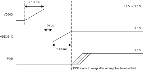
When VDDIO and VDD33_X are powered separately, the VDDIO supply (1.8 V or 3.3 V) ramps up 100 µs before the other supply (VDD33_X) begins to ramp. If VDDIO is tied with VDD33_X, both supplies may ramp at the same time. The VDDs (VDD33_X and VDDIO) supply ramp must be faster than 1.5 ms with a monotonic rise. Use a large capacitor on the PDB pin to ensure PDB arrives after all the VDDs have settled to the recommended operating voltage. When PDB pin is pulled to VDDIO = 3 V to 3.6 V or VDD33_X, TI recommends using a 10-kΩ pullup and a > 10-µF cap to GND to delay the PDB input signal.
All inputs must not be driven until VDD33_X and VDDIO has reached its steady-state value.
 Figure 28. Power-Up Sequence of DS90UH926Q-Q1