SNOSCZ4 April 2015
PRODUCTION DATA.
- 1 Features
- 2 Applications
- 3 Description
- 4 Typical Application
- 5 Revision History
- 6 Pin Configuration and Functions
- 7 Specifications
- 8 Detailed Description
- 9 Applications and Implementation
- 10Power Supply Recommendations
- 11Layout
- 12Device and Documentation Support
- 13Mechanical, Packaging, and Orderable Information
Package Options
Mechanical Data (Package|Pins)
- DGS|10
Thermal pad, mechanical data (Package|Pins)
Orderable Information
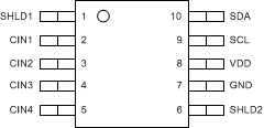
6 Pin Configuration and Functions
DGS Package
10 Pin VSSOP
Top View

Pin Functions
| PIN | TYPE(1) | DESCRIPTION | |
|---|---|---|---|
| NAME | NO. | ||
| SHLD1 | 1 | A | Capacitive Input Active AC Shielding. |
| CIN1 | 2 | A | Capacitive Input. The measured capacitance is connected between the CIN1 pin and GND. If not used, this pin should be left as an open circuit. |
| CIN2 | 3 | A | Capacitive Input. The measured capacitance is connected between the CIN2 pin and GND. If not used, this pin should be left as an open circuit. |
| CIN3 | 4 | A | Capacitive Input. The measured capacitance is connected between the CIN3 pin and GND. If not used, this pin should be left as an open circuit. |
| CIN4 | 5 | A | Capacitive Input. The measured capacitance is connected between the CIN4 pin and GND. If not used, this pin should be left as an open circuit. |
| SHLD2 | 6 | A | Capacitive Input Active AC Shielding. |
| GND | 7 | G | Ground |
| VDD | 8 | P | Power Supply Voltage. This pin should be decoupled to GND, using a low impedance capacitor, for example in combination with a 1-μF tantalum and a 0.1-μF multilayer ceramic. |
| SCL | 9 | I | Serial Interface Clock Input. Connects to the master clock line. Requires pull-up resistor if not already provided elsewhere in the system. |
| SDA | 10 | I/O | Serial Interface Bidirectional Data. Connects to the master data line. Requires a pull-up resistor if not provided elsewhere in the system. |
(1) P=Power, G=Ground, I=Input, O=Output, A=Analog, I/O=Bi-Directional Input/Output