SBOS062C September 2000 – January 2022 INA126 , INA2126
PRODUCTION DATA
- 1 Features
- 2 Applications
- 3 Description
- 4 Revision History
- 5 Pin Configuration and Functions
- 6 Specifications
- 7 Detailed Description
- 8 Application and Implementation
- 9 Power Supply Recommendations
- 10Layout
- 11Device and Documentation Support
- 12Mechanical, Packaging, and Orderable Information
Package Options
Mechanical Data (Package|Pins)
Thermal pad, mechanical data (Package|Pins)
- D|8
Orderable Information
8.2.3 Application Curves

Differential
signal is too small to be seen
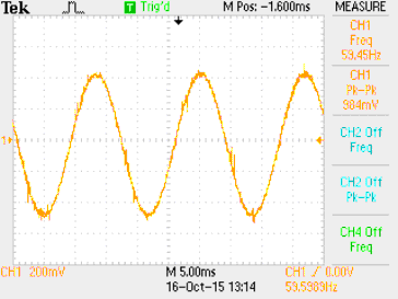
Figure 8-4 Common-mode Signal at
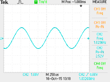
INA126 Input Figure 8-6 Recovered Differential Signal at the Output of the INA126 With a Gain of
250
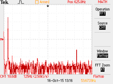
 Figure 8-5 FFT of Signal in Previous
Figure Shows Both the 60-Hz Common-mode Along With 5-kHz Differential
Signal
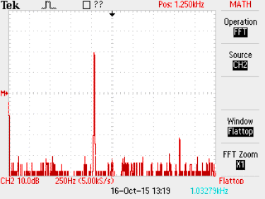
 Figure 8-7 FFT
of the INA126 Output Shows that the 60-Hz Common-mode Signal is
Rejected