SBOS051F October   1995  – May 2022 INA128 , INA129

PRODUCTION DATA  

  1. Features
  2. Applications
  3. Description
  4. Revision History
  5. Device Comparison Table
  6. Pin Configuration and Functions
  7. Specifications
    1. 7.1 Absolute Maximum Ratings
    2. 7.2 ESD Ratings
    3. 7.3 Recommended Operating Conditions
    4. 7.4 Thermal Information
    5. 7.5 Electrical Characteristics
    6. 7.6 Typical Characteristics
  8. Detailed Description
    1. 8.1 Overview
    2. 8.2 Functional Block Diagram
    3. 8.3 Feature Description
      1. 8.3.1 Noise Performance
    4. 8.4 Device Functional Modes
  9. Application and Implementation
    1. 9.1 Application Information
      1. 9.1.1 Input Common-Mode Range
    2. 9.2 Typical Application
      1. 9.2.1 Design Requirements
      2. 9.2.2 Detailed Design Procedure
        1. 9.2.2.1 Setting the Gain
        2. 9.2.2.2 Dynamic Performance
        3. 9.2.2.3 Offset Trimming
        4. 9.2.2.4 Input Bias Current Return Path
      3. 9.2.3 Application Curves
    3. 9.3 System Examples
  10. 10Power Supply Recommendations
    1. 10.1 Low-Voltage Operation
  11. 11Layout
    1. 11.1 Layout Guidelines
    2. 11.2 Layout Example
  12. 12Device and Documentation Support
    1. 12.1 Device Support
      1. 12.1.1 Development Support
        1. 12.1.1.1 PSpice® for TI
        2. 12.1.1.2 TINA-TI™ Simulation Software (Free Download)
    2. 12.2 Documentation Support
      1. 12.2.1 Related Documentation
    3. 12.3 Receiving Notification of Documentation Updates
    4. 12.4 Support Resources
    5. 12.5 Trademarks
    6. 12.6 Electrostatic Discharge Caution
    7. 12.7 Glossary
  13. 13Mechanical, Packaging, and Orderable Information

Package Options

Mechanical Data (Package|Pins)
Thermal pad, mechanical data (Package|Pins)
Orderable Information

Typical Characteristics

at TA = 25°C, VS = ±15 V, RL = 10 kΩ, VREF = 0 V, VCM = VS / 2, and G = 1 (unless otherwise noted)
GUID-20220214-SS0I-3R6S-PLCB-2RZZF23HCXSV-low.png
 
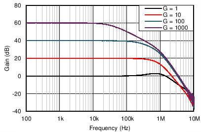
Figure 7-1 Gain vs Frequency
 
Figure 7-3 Positive Power Supply Rejection vs Frequency
GUID-4490F525-FB74-42EF-9761-33BB8445F87B-low.gif
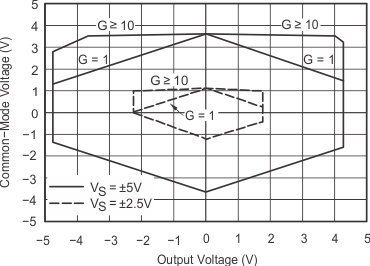
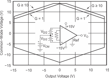
VS = ±15 V
Figure 7-5 Input Common-Mode Range vs Output Voltage
 
Figure 7-7 Input-Referred Noise vs Frequency
 
Figure 7-9 Quiescent Current vs Temperature
 
Figure 7-11 Input Offset Voltage Warm-Up
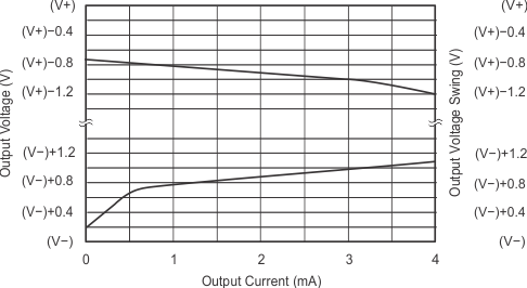
GUID-02F5E9B6-A259-4FC7-B4AF-8E6E3B7710E3-low.gif
 
 
Figure 7-13 Output Voltage Swing vs Output Current
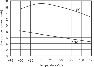
GUID-EC182392-B2E4-4D11-996B-09D8C0BC3D65-low.gif
 
Figure 7-15 Short Circuit Output Current vs Temperature
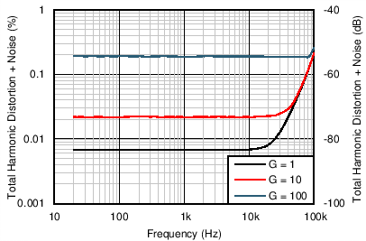
GUID-20220214-SS0I-CXTD-ZHLT-MHR8NRSRQ1LZ-low.png
 
Figure 7-17 Total Harmonic Distortion + Noise vs Frequency
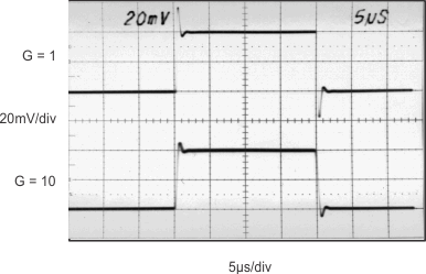
GUID-5EABEEE5-2316-4805-97C4-E6AD8C1C3D6F-low.gif
  G = 1, 10
Figure 7-19 Small Signal
  G = 1, 10
Figure 7-21 Large Signal
GUID-87480DDD-5B88-4B96-BAC1-D947CCF2C601-low.gif
 
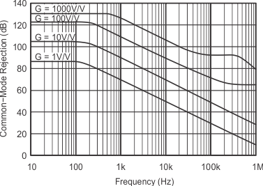
Figure 7-2 Common-Mode Rejection vs Frequency
GUID-20220214-SS0I-DKTW-XLPD-GLDR4LFRFPGH-low.png
 
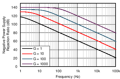
Figure 7-4 Negative Power Supply Rejection vs Frequency
GUID-A7440062-EA47-4620-AA96-77BCD406BCF1-low.gif
VS = ±5 V, ±2.5 V
Figure 7-6 Input Common-Mode Range vs Output Voltage
GUID-A8600F34-C11D-4F34-B066-530BE3C6C006-low.gif
 
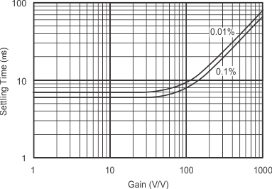
Figure 7-8 Settling Time vs Gain
GUID-20220214-SS0I-NLHX-80K0-NFJBHS2MNT3H-low.png
 
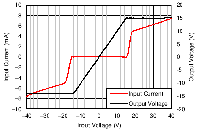
Figure 7-10 Input Overvoltage V/I Characteristics
GUID-AB71D8E9-6120-4305-BF59-C358E916FB8D-low.gif
 
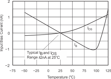
Figure 7-12 Input Bias Current vs Temperature
GUID-179E0688-C831-4F50-85DC-4D04924ACD55-low.gif
 
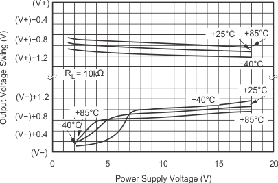
Figure 7-14 Output Voltage Swing vs Power Supply Voltage
GUID-20220214-SS0I-DF4X-WBWK-0C18ZWP0THFM-low.png
 
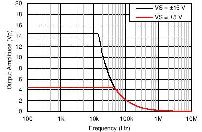
Figure 7-16 Maximum Output Voltage vs Frequency
GUID-6F1356BF-BDC2-47F7-8A10-5A0E8C89D396-low.gif
  G ≥ 100
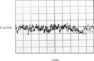
Figure 7-18 0.1 to 10-Hz Input-Referred Voltage Noise
GUID-47FDD2C5-2310-482B-82D1-CF2292FD0346-low.gif
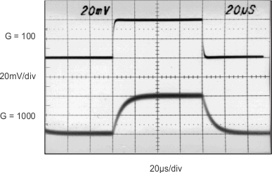
  G = 100, 1000
Figure 7-20 Small Signal
  G = 100, 1000
Figure 7-22 Large Signal