SBOS772C August 2017 – May 2019 INA1650-Q1 , INA1651-Q1
PRODUCTION DATA.
- 1 Features
- 2 Applications
- 3 Description
- 4 Revision History
- 5 Pin Configuration and Functions
- 6 Specifications
- 7 Detailed Description
- 8 Application and Implementation
- 9 Power Supply Recommendations
- 10Layout
- 11Device and Documentation Support
- 12Mechanical, Packaging, and Orderable Information
Package Options
Mechanical Data (Package|Pins)
- PW|14
Thermal pad, mechanical data (Package|Pins)
- PW|14
Orderable Information
7.3.4 Electrical Overstress
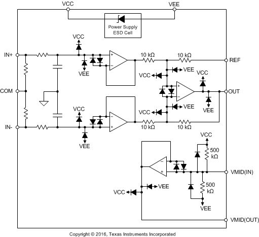
Designers often ask questions about the capability of an amplifier to withstand electrical overstress. These questions typically focus on the device inputs, but can involve the supply voltage pins or the output pin. Each of these different pin functions have electrical stress limits determined by the voltage breakdown characteristics of the particular semiconductor fabrication process and specific circuits connected to the pin. Additionally, internal electrostatic discharge (ESD) protection is built into these circuits to protect them from accidental ESD events, both before and during product assembly. A good understanding of basic ESD circuitry and the relevance of circuitry to an electrical overstress event is helpful. Figure 43 illustrates the ESD circuits contained in the INA165x-Q1. The ESD protection circuitry involves several current-steering diodes that are connected from the input and output pins, and routed back to the internal power-supply lines. This protection circuitry is intended to remain inactive during normal circuit operation. The input pins of the INA165x-Q1 are protected with internal diodes that are connected to the power-supply rails. These diodes clamp the applied signal to prevent the input circuitry from damage. If the input signal voltage exceeds the power supplies by more than 0.3 V, limit the input signal current to less than 10 mA to protect the internal clamp diodes. A series input resistor can typically limit the current. Some signal sources are inherently current-limited and do not require limiting resistors.
 Figure 43. INA165x-Q1 Internal ESD Protection Circuitry
(Single Channel and Supply-Divider Shown for Simplicity)