SBOS741H April 2017 – July 2022 INA180 , INA2180 , INA4180
PRODUCTION DATA
- 1 Features
- 2 Applications
- 3 Description
- 4 Revision History
- 5 Device Comparison
- 6 Pin Configuration and Functions
- 7 Specifications
- 8 Detailed Description
- 9 Application and Implementation
- 10Device and Documentation Support
Package Options
Mechanical Data (Package|Pins)
- DBV|5
Thermal pad, mechanical data (Package|Pins)
Orderable Information
9.1.2 RSENSE and Device Gain Selection
The accuracy of the INAx180 is maximized by choosing the current-sense resistor to be as large as possible. A large sense resistor maximizes the differential input signal for a given amount of current flow and reduces the error contribution of the offset voltage. However, there are practical limits as to how large the current-sense resistor can be in a given application. The INAx180 have a typical input bias currents of 80 µA for each input when operated at a 12-V common-mode voltage input. When large current-sense resistors are used, these bias currents cause increased offset error and reduced common-mode rejection. Therefore, using current-sense resistors larger than a few ohms is generally not recommended for applications that require current-monitoring accuracy. A second common restriction on the value of the current-sense resistor is the maximum allowable power dissipation that is budgeted for the resistor. Equation 1 gives the maximum value for the current sense resistor for a given power dissipation budget:
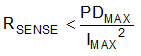
where:
- PDMAX is the maximum allowable power dissipation in RSENSE.
- IMAX is the maximum current that will flow through RSENSE.
An additional limitation on the size of the current-sense resistor and device gain is due to the power-supply voltage, VS, and device swing to rail limitations. In order to make sure that the current-sense signal is properly passed to the output, both positive and negative output swing limitations must be examined. Equation 2 provides the maximum values of RSENSE and GAIN to keep the device from hitting the positive swing limitation.
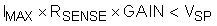
where:
- IMAX is the maximum current that will flow through RSENSE.
- GAIN is the gain of the current sense-amplifier.
- VSP is the positive output swing as specified in the data sheet.
To avoid positive output swing limitations when selecting the value of RSENSE, there is always a trade-off between the value of the sense resistor and the gain of the device under consideration. If the sense resistor selected for the maximum power dissipation is too large, then it is possible to select a lower-gain device in order to avoid positive swing limitations.
The negative swing limitation places a limit on how small of a sense resistor can be used in a given application. Equation 3 provides the limit on the minimum size of the sense resistor.
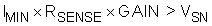
where:
- IMIN is the minimum current that will flow through RSENSE.
- GAIN is the gain of the current sense amplifier.
- VSN is the negative output swing of the device (see Section 8.3.4).