SBOS318B April 2019 – July 2021 INA186
PRODUCTION DATA
- 1 Features
- 2 Applications
- 3 Description
- 4 Revision History
- 5 Pin Configuration and Functions
- 6 Specifications
- 7 Detailed Description
- 8 Application and Implementation
- 9 Power Supply Recommendations
- 10Layout
- 11Device and Documentation Support
- 12Mechanical, Packaging, and Orderable Information
Package Options
Refer to the PDF data sheet for device specific package drawings
Mechanical Data (Package|Pins)
- DDF|8
- YFD|6
- DCK|6
Thermal pad, mechanical data (Package|Pins)
- DCK|6
Orderable Information
3 Description
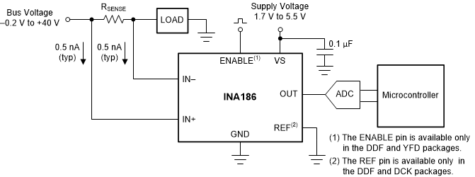
The INA186 is a low-power, voltage-output, current-sense amplifier (also called a current-shunt monitor). This device is commonly used for overcurrent protection, precision current measurement for system optimization, or in closed-loop feedback circuits. The INA186 can sense drops across shunts at common-mode voltages from –0.2 V to +40 V, independent of the supply voltage.
The low input bias current of the INA186 permits the use of larger current-sense resistors, thus providing accurate current measurements in the microamp range. The low offset voltage of the zero-drift architecture extends the dynamic range of the current measurement. This feature allows for smaller sense resistors with lower power loss, while still providing accurate current measurements.
The INA186 operates from a single 1.7-V to 5.5-V power supply, and draws a maximum of 90 μA of supply current . Five fixed gain options are available: 25 V/V, 50 V/V, 100 V/V, 200 V/V, or 500 V/V. The device is specified over the operating temperature range of –40°C to +125°C, and offered in SC70, SOT-23-THIN, and DSBGA packages. The SC70 and SOT-23 (DDF) packages support bidirectional current measurement, whereas the DSBGA package only supports current measurement in one direction.
| PART NUMBER | PACKAGE(1) | BODY SIZE (NOM) |
|---|---|---|
| INA186 | SC70 (6) | 2.00 mm × 1.25 mm |
| SOT-23 (8) | 2.90 mm × 1.60 mm | |
| DSBGA (6) | 1.17 mm × 0.765 mm |
 Typical Application