SBOS318B April 2019 – July 2021 INA186
PRODUCTION DATA
- 1 Features
- 2 Applications
- 3 Description
- 4 Revision History
- 5 Pin Configuration and Functions
- 6 Specifications
- 7 Detailed Description
- 8 Application and Implementation
- 9 Power Supply Recommendations
- 10Layout
- 11Device and Documentation Support
- 12Mechanical, Packaging, and Orderable Information
Package Options
Refer to the PDF data sheet for device specific package drawings
Mechanical Data (Package|Pins)
- DDF|8
- YFD|6
- DCK|6
Thermal pad, mechanical data (Package|Pins)
- DCK|6
Orderable Information
8.1.4 Common-Mode Voltage Transients
With a small amount of additional circuitry, the
INA186 can be used in circuits subject to transients that
exceed the absolute maximum voltage ratings. The most simple way to protect the
inputs from negative transients is to add resistors in series with the IN– and IN+
pins. Use resistors that are 1 kΩ or less, and limit the current in the ESD
structures to less than 5 mA. For example, using 1-kΩ resistors in series with the
INA186 allows voltages as low as –5 V, while limiting the ESD
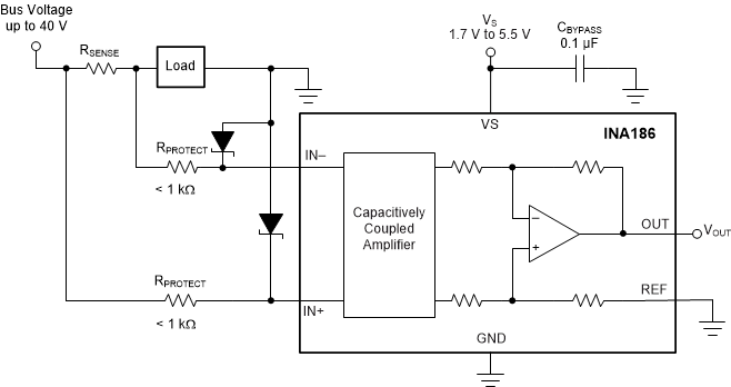
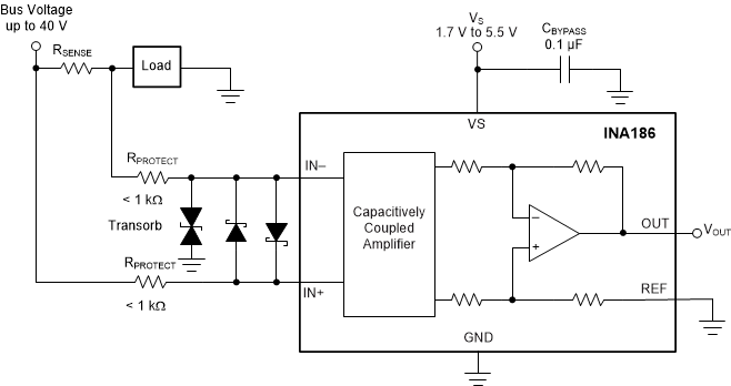
current to less than 5 mA. Use the circuits shown in Figure 8-4 and Figure 8-5 if protection from high-voltage or more-negative, common-voltage transients is
needed. When implementing these circuits, use only Zener diodes or Zener-type
transient absorbers (sometimes referred to as transzorbs); any other type of
transient absorber has an unacceptable time delay. Start by adding a pair of
resistors as a working impedance for the Zener diode (see Figure 8-4). Keep these resistors as small as possible; most often, use around 100 Ω. See
Section 8.1.3 for information on how larger values can be used with an effect on gain.
This circuit limits only short-term transients; therefore, many applications are
satisfied with a 100-Ω resistor along with conventional Zener diodes of the lowest
acceptable power rating. This combination uses the least amount of board space.
These diodes can be found in packages as small as
SOT-523 or SOD-523.
 Figure 8-4 Transient Protection Using Dual Zener Diodes
In the event that low-power Zener diodes do not have sufficient transient absorption capability, a higher-power transzorb must be used. The most package-efficient solution involves using a single transzorb and back-to-back diodes between the device inputs, as shown in Figure 8-5. The most space-efficient solutions are dual, series-connected diodes in a single SOT-523 or SOD-523 package. In either of the examples shown in Figure 8-4 and Figure 8-5, the total board area required by the INA186 with all protective components is less than that of an SO-8 package, and only slightly greater than that of an VSSOP-8 package.
 Figure 8-5 Transient Protection Using a Single Transzorb and Input Clamps
For more information, see the Current Shunt Monitor With Transient Robustness reference design.