SBOS318B April 2019 – July 2021 INA186
PRODUCTION DATA
- 1 Features
- 2 Applications
- 3 Description
- 4 Revision History
- 5 Pin Configuration and Functions
- 6 Specifications
- 7 Detailed Description
- 8 Application and Implementation
- 9 Power Supply Recommendations
- 10Layout
- 11Device and Documentation Support
- 12Mechanical, Packaging, and Orderable Information
Package Options
Refer to the PDF data sheet for device specific package drawings
Mechanical Data (Package|Pins)
- DDF|8
- YFD|6
- DCK|6
Thermal pad, mechanical data (Package|Pins)
- DCK|6
Orderable Information
7.4.3 Bidirectional Mode
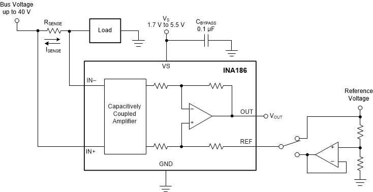
The INA186 is a bidirectional current-sense amplifier capable of measuring currents through a resistive shunt in two directions. This bidirectional monitoring is common in applications that include charging and discharging operations where the current flowing through the resistor can change directions.
 Figure 7-4 Bidirectional Application
By applying a voltage to the REF pin, Figure 7-4 shows how you can measure this current flowing in both directions. The voltage applied to REF (VREF) sets the output state that corresponds to the zero-input level state. The output then responds by increasing above VREF for positive differential signals (relative to the IN– pin) and responds by decreasing below VREF for negative differential signals. This reference voltage applied to the REF pin can be set anywhere between 0 V to VS. For bidirectional applications, VREF is typically set at VS/2 for equal signal range in both current directions. In some cases, VREF is set at a voltage other than VS/2; for example, when the bidirectional current and corresponding output signal do not need to be symmetrical.