SBOS632 September 2015 INA188
UNLESS OTHERWISE NOTED, this document contains PRODUCTION DATA.
- 1 Features
- 2 Applications
- 3 Description
- 4 Revision History
- 5 Pin Configuration and Functions
- 6 Specifications
- 7 Detailed Description
- 8 Application and Implementation
- 9 Power Supply Recommendations
- 10Layout
- 11Device and Documentation Support
- 12Mechanical, Packaging, and Orderable Information
Package Options
Mechanical Data (Package|Pins)
Thermal pad, mechanical data (Package|Pins)
- DRJ|8
Orderable Information
1 Features
- Excellent DC Performance:
- Low Input Offset Voltage: 55 μV (max)
- Low Input Offset Drift: 0.2 μV/°C (max)
- High CMRR: 104 dB, G ≥ 10 (min)
- Low Input Noise:
- 12 nV/√Hz at 1 kHz
- 0.25 μVPP (0.1 Hz to 10 Hz)
- Wide Supply Range:
- Single Supply: 4 V to 36 V
- Dual Supply: ±2 V to ±18 V
- Gain Set with a Single External Resistor:
- Gain Equation: G = 1 + (50 kΩ / RG)
- Gain Error: 0.007%, G = 1
- Gain Drift: 5 ppm/°C (max) G = 1
- Input Voltage: (V–) + 0.1 V to (V+) – 1.5 V
- RFI-Filtered Inputs
- Rail-to-Rail Output
- Low Quiescent Current: 1.4 mA
- Operating Temperature: –55°C to +150°C
- SOIC-8 and DFN-8 Packages
2 Applications
- Bridge Amplifiers
- ECG Amplifiers
- Pressure Sensors
- Medical Instrumentation
- Portable Instrumentation
- Weigh Scales
- Thermocouple Amplifiers
- RTD Sensor Amplifiers
- Data Acquisition
3 Description
The INA188 is a precision instrumentation amplifier that uses TI proprietary auto-zeroing techniques to achieve low offset voltage, near-zero offset and gain drift, excellent linearity, and exceptionally low-noise density (12 nV/√Hz) that extends down to dc.
The INA188 is optimized to provide excellent common-mode rejection of greater than 104 dB (G ≥ 10). Superior common-mode and supply rejection supports high-resolution, precise measurement applications. The versatile three op-amp design offers a rail-to-rail output, low-voltage operation from a 4-V single supply as well as dual supplies up to ±18 V, and a wide, high-impedance input range. These specifications make this device ideal for universal signal measurement and sensor conditioning (such as temperature or bridge applications).
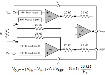
A single external resistor sets any gain from 1 to 1000. The INA188 is designed to use an industry-standard gain equation: G = 1 + (50 kΩ / RG). The reference pin can be used for level-shifting in single-supply operation or for an offset calibration.
The INA188 is specified over the temperature range of –40°C to +125°C .
Device Information
| ORDER NUMBER | PACKAGE | BODY SIZE |
|---|---|---|
| INA188 | SOIC (8) | 4.90 mm × 3.91 mm |
| INA188 | WSON (8)(2) | 4.00 mm × 4.00 mm |
- For all available packages, see the orderable addendum at the end of the data sheet.
- The DRJ package (WSON-8) is a preview device.
Simplified Schematic
