SBOS366E August 2006 – January 2021 INA193A-Q1 , INA194A-Q1 , INA195A-Q1 , INA196A-Q1 , INA197A-Q1 , INA198A-Q1
PRODUCTION DATA
- 1 Features
- 2 Applications
- 3 Description
- 4 Revision History
- 5 Pin Configuration and Functions
- 6 Specifications
- 7 Detailed Description
- 8 Application and Implementation
- 9 Power Supply Recommendations
- 10Layout
- 11Device and Documentation Support
- 12Mechanical, Packaging, and Orderable Information
Package Options
Mechanical Data (Package|Pins)
- DBV|5
Thermal pad, mechanical data (Package|Pins)
Orderable Information
7.4.2.3 Low VSENSE Case 1: VSENSE < 20 mV, –16 V ≤ VCM < 0; and Low VSENSE Case 3: VSENSE < 20 mV,
VS < VCM ≤ 80 V
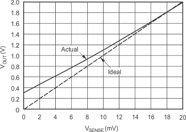
Although the INA19xA-Q1 family of devices are not designed for accurate operation in either of these regions, some applications are exposed to these conditions; for example, when monitoring power supplies that are switched on and off while VS is still applied to the INA19xA-Q1. It is important to know what the behavior of the devices will be in these regions.
As VSENSE approaches 0 mV, in these
VCM regions, the device output accuracy degrades. A
larger-than-normal offset can appear at the current shunt monitor output with a
typical maximum value of VOUT = 300 mV for
VSENSE = 0 mV. As VSENSE approaches 20 mV, VOUT
returns to the expected output value with accuracy as specified in Electrical Characteristics. Figure 7-7 illustrates this effect using the INA195A and INA198A
(Gain = 100).
 Figure 7-7 Example for Low VSENSE Cases 1 and 3 (INA195A-Q1, INA198A-Q1: Gain = 100)