SBOS366E August   2006  – January 2021 INA193A-Q1 , INA194A-Q1 , INA195A-Q1 , INA196A-Q1 , INA197A-Q1 , INA198A-Q1

PRODUCTION DATA  

  1. Features
  2. Applications
  3. Description
  4. Revision History
  5. Pin Configuration and Functions
  6. Specifications
    1. 6.1 Absolute Maximum Ratings
    2. 6.2 ESD Ratings
    3. 6.3 Recommended Operating Conditions
    4. 6.4 Thermal Information
    5. 6.5 Electrical Characteristics
    6. 6.6 Typical Characteristics
  7. Detailed Description
    1. 7.1 Overview
    2. 7.2 Functional Block Diagram
    3. 7.3 Feature Description
      1. 7.3.1 Basic Connection
      2. 7.3.2 Selecting RS
      3. 7.3.3 Inside the INA19xA
      4. 7.3.4 Power Supply
    4. 7.4 Device Functional Modes
      1. 7.4.1 Input Filtering
      2. 7.4.2 Accuracy Variations as a Result Of VSENSE and Common Mode Voltage
        1. 7.4.2.1 Normal Case 1: VSENSE ≥ 20 mV, VCM ≥ VS
        2. 7.4.2.2 Normal Case 2: VSENSE ≥ 20 mV, VCM < VS
        3. 7.4.2.3 Low VSENSE Case 1: VSENSE < 20 mV, –16 V ≤ VCM < 0; and Low VSENSE Case 3: VSENSE < 20 mV, VS < VCM ≤ 80 V
        4. 7.4.2.4 Low VSENSE Case 2: VSENSE < 20 mV, 0 V ≤ VCM ≤ VS
      3. 7.4.3 Shutdown
      4. 7.4.4 Transient Protection
      5. 7.4.5 Output Voltage Range
  8. Application and Implementation
    1. 8.1 Application Information
    2. 8.2 Typical Application
      1. 8.2.1 Design Requirements
      2. 8.2.2 Detailed Design Procedure
      3. 8.2.3 Application Curve
  9. Power Supply Recommendations
  10. 10Layout
    1. 10.1 Layout Guidelines
      1. 10.1.1 RFI/EMI
    2. 10.2 Layout Example
  11. 11Device and Documentation Support
    1. 11.1 Receiving Notification of Documentation Updates
    2. 11.2 Support Resources
    3. 11.3 Trademarks
    4. 11.4 Electrostatic Discharge Caution
    5. 11.5 Glossary
  12. 12Mechanical, Packaging, and Orderable Information

Package Options

Mechanical Data (Package|Pins)
Thermal pad, mechanical data (Package|Pins)
Orderable Information

Description

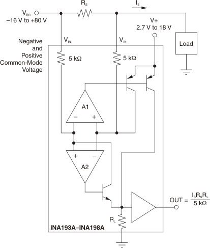
The INA19xA-Q1 family of current shunt monitors with voltage output can sense drops across shunts at common-mode voltages from –16 V to 80 V, independent of the INA19xA supply voltage. They are available with three output voltage scales: 20 V/V, 50 V/V, and 100 V/V. The 500-kHz bandwidth simplifies use in current control loops and monitoring DC motor health. The INA193A–INA195A provide identical functions but alternative pin configurations to the INA196A–INA198A, respectively.

The INA19xA-Q1 operate from a single 2.7-V to 18-V supply. They are specified over the extended operating temperature range (–40°C to 125°C), and are offered in a space-saving SOT-23 package.

Device Information(1)
PART NUMBERPACKAGEBODY SIZE (NOM)
INA19xA-Q1SOT-23 (5)2.90 mm × 1.60 mm
For all available packages, see the package option addendum at the end of the data sheet.
GUID-71F036FF-5F43-4512-B510-9AE6D137FEF2-low.gifSimplified Schematic