SBOS366E August 2006 – January 2021 INA193A-Q1 , INA194A-Q1 , INA195A-Q1 , INA196A-Q1 , INA197A-Q1 , INA198A-Q1
PRODUCTION DATA
- 1 Features
- 2 Applications
- 3 Description
- 4 Revision History
- 5 Pin Configuration and Functions
- 6 Specifications
- 7 Detailed Description
- 8 Application and Implementation
- 9 Power Supply Recommendations
- 10Layout
- 11Device and Documentation Support
- 12Mechanical, Packaging, and Orderable Information
Package Options
Mechanical Data (Package|Pins)
- DBV|5
Thermal pad, mechanical data (Package|Pins)
Orderable Information
6.6 Typical Characteristics
TA = 25°C, VS = 12 V, VIN+ = 12 V, and VSENSE = 100 mV (unless otherwise noted)
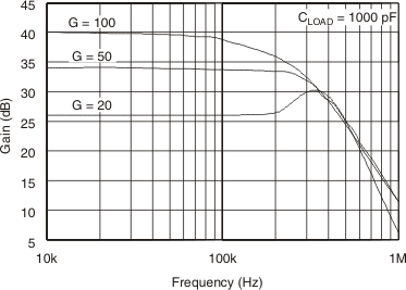 Figure 6-1 Gain vs Frequency
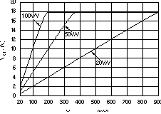 Figure 6-3 Gain
Plot
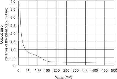 Figure 6-5 Output Error vs Vsense
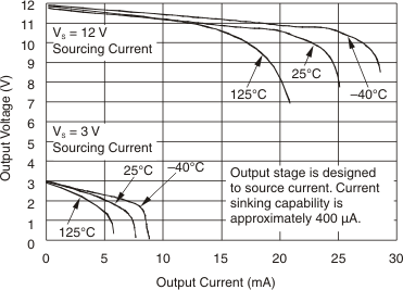 Figure 6-7 Positive Output Voltage Swing vs Output Current
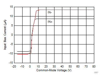
| Vs=5 V |
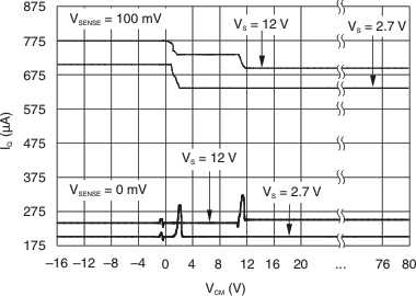 Figure 6-11 Quiescent Current vs Common Mode Voltage
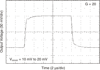 Figure 6-13 Step
Response
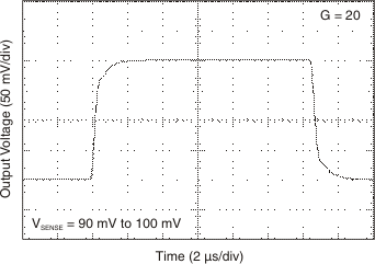 Figure 6-15 Step
Response
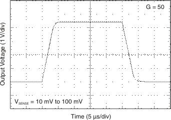 Figure 6-17 Step
Response
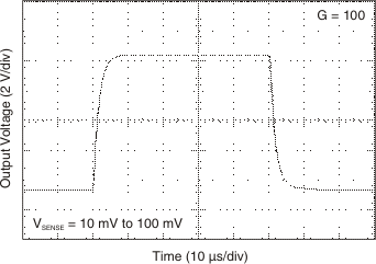 Figure 6-19 Step
Response
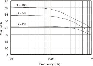 Figure 6-2 Gain vs Frequency
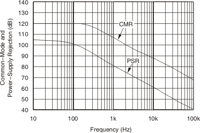 Figure 6-4 Common-Mode and Power-Supply Rejection vs Frequency
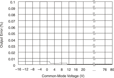 Figure 6-6 Output Error vs Common-Mode Voltage
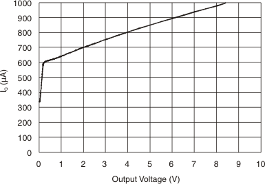 Figure 6-8 Quiescent Current vs Output Voltage
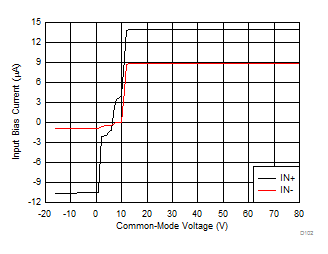
| Vs =12 V |
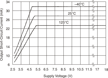 Figure 6-12 Output Short Circuit Current vs Supply Voltage
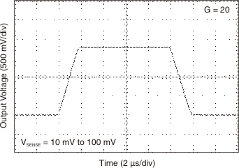 Figure 6-14 Step
Response
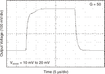 Figure 6-16 Step
Response
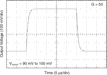 Figure 6-18 Step
Response