SBOS781E March   2016  – May 2021 INA199-Q1

PRODUCTION DATA  

  1. Features
  2. Applications
  3. Description
  4. Revision History
  5. Device Comparison
  6. Pin Configuration and Functions
  7. Specifications
    1. 7.1 Absolute Maximum Ratings
    2. 7.2 ESD Ratings
    3. 7.3 Recommended Operating Conditions
    4. 7.4 Thermal Information
    5. 7.5 Electrical Characteristics
    6. 7.6 Typical Characteristics
  8. Detailed Description
    1. 8.1 Overview
    2. 8.2 Functional Block Diagram
    3. 8.3 Feature Description
      1. 8.3.1 Zero-Drift Offset
      2. 8.3.2 Accuracy
      3. 8.3.3 Choice of Gain Options
    4. 8.4 Device Functional Modes
  9. Application and Implementation
    1. 9.1 Application Information
      1. 9.1.1 Basic Connections
      2. 9.1.2 Input Filtering
      3. 9.1.3 Shutting Down the INA199-Q1
      4. 9.1.4 REF Input Impedance Effects
      5. 9.1.5 Using the INA199-Q1 With Common-Mode Transients Above 26 V
    2. 9.2 Typical Applications
      1. 9.2.1 Unidirectional Operation
        1. 9.2.1.1 Design Requirements
        2. 9.2.1.2 Detailed Design Procedure
        3. 9.2.1.3 Application Curve
      2. 9.2.2 Bidirectional Operation
        1. 9.2.2.1 Design Requirements
        2. 9.2.2.2 Detailed Design Procedure
        3. 9.2.2.3 Application Curve
  10. 10Power Supply Recommendations
  11. 11Layout
    1. 11.1 Layout Guidelines
    2. 11.2 Layout Example
  12. 12Device and Documentation Support
    1. 12.1 Documentation Support
      1. 12.1.1 Related Documentation
    2. 12.2 Receiving Notification of Documentation Updates
    3. 12.3 Support Resources
    4. 12.4 Trademarks
    5. 12.5 Electrostatic Discharge Caution
    6. 12.6 Glossary
  13. 13Mechanical, Packaging, and Orderable Information

Package Options

Mechanical Data (Package|Pins)
Thermal pad, mechanical data (Package|Pins)
Orderable Information

Application Curve

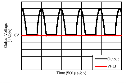
An example output response of a unidirectional configuration is shown in Figure 9-8. With the REF pin connected directly to ground, the output voltage is biased to this zero output level. The output rises above the reference voltage for positive differential input signals but cannot fall below the reference voltage for negative differential input signals because of the grounded reference voltage.
GUID-729EE7C3-74C7-4D26-B591-3708C4834C1C-low.pngFigure 9-8 Unidirectional Application Output Response