SBOS393F March 2007 – June 2021 INA203 , INA204 , INA205
PRODUCTION DATA
- 1 Features
- 2 Applications
- 3 Description
- 4 Revision History
- 5 Pin Configuration and Functions
-
6 Specifications
- 6.1 Absolute Maximum Ratings
- 6.2 ESD Ratings
- 6.3 Recommended Operating Conditions
- 6.4 Thermal Information
- 6.5 Electrical Characteristics: Current-Shunt Monitor
- 6.6 Electrical Characteristics: Comparator
- 6.7 Electrical Characteristics: Reference
- 6.8 Electrical Characteristics: General
- 6.9 Typical Characteristics
- 7 Detailed Description
- 8 Application and Implementation
- 9 Power Supply Recommendations
- 10Layout
- 11Device and Documentation Support
- 12Mechanical, Packaging, and Orderable Information
Package Options
Refer to the PDF data sheet for device specific package drawings
Mechanical Data (Package|Pins)
- D|14
- DGS|10
- PW|14
Thermal pad, mechanical data (Package|Pins)
Orderable Information
7.4.2.1 Normal Case 1: VSENSE ≥ 20 mV, VCM ≥ VS
This region of operation provides the highest accuracy. Here, the input offset voltage is characterized and measured using a two-step method. First, the gain is determined by Equation 3.

where
- VOUT1 = Output Voltage with VSENSE = 100 mV.
- VOUT2 = Output Voltage with VSENSE = 20 mV.
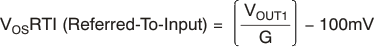
Then the offset voltage is measured at VSENSE = 100 mV and referred to the input (RTI) of the current shunt monitor, as shown in Equation 4.
In the Section 6.9, Figure 6-7 shows the highest accuracy for this region of operation. In this plot, VS = 12 V; for VCM ≥ 12 V, the output error is at its minimum. This case is also used to create the VSENSE ≥ 20-mV output specifications in the Section 6.5 table.