SBOS393F March 2007 – June 2021 INA203 , INA204 , INA205
PRODUCTION DATA
- 1 Features
- 2 Applications
- 3 Description
- 4 Revision History
- 5 Pin Configuration and Functions
-
6 Specifications
- 6.1 Absolute Maximum Ratings
- 6.2 ESD Ratings
- 6.3 Recommended Operating Conditions
- 6.4 Thermal Information
- 6.5 Electrical Characteristics: Current-Shunt Monitor
- 6.6 Electrical Characteristics: Comparator
- 6.7 Electrical Characteristics: Reference
- 6.8 Electrical Characteristics: General
- 6.9 Typical Characteristics
- 7 Detailed Description
- 8 Application and Implementation
- 9 Power Supply Recommendations
- 10Layout
- 11Device and Documentation Support
- 12Mechanical, Packaging, and Orderable Information
Package Options
Refer to the PDF data sheet for device specific package drawings
Mechanical Data (Package|Pins)
- D|14
- DGS|10
- PW|14
Thermal pad, mechanical data (Package|Pins)
Orderable Information
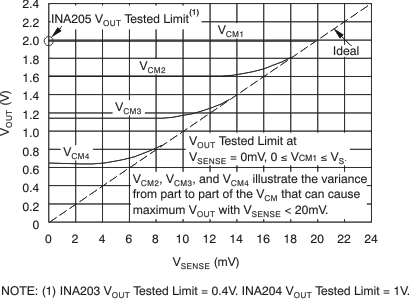
7.4.2.4 Low VSENSE Case 2: VSENSE < 20 mV, 0 V ≤ VCM ≤ VS
This region of operation is the least accurate for the INA203 family. To achieve the wide input common-mode voltage range, these devices use two op amp front ends in parallel. One operational amplifier front end operates in the positive input common-mode voltage range, and the other in the negative input region. For this case, neither of these two internal amplifiers dominates and overall loop gain is very low. Within this region, VOUT approaches voltages close to linear operation levels for Normal Case 2. This deviation from linear operation becomes greatest the closer VSENSE approaches 0 V. Within this region, as VSENSE approaches 20 mV, device operation is closer to that described by Normal Case 2. Figure 7-12 illustrates this behavior for the INA205. The VOUT maximum peak for this case is tested by maintaining a constant VS, setting VSENSE = 0 mV, and sweeping VCM from 0 V to VS. The exact VCM at which VOUT peaks during this test varies from part to part, but the VOUT maximum peak is tested to be less than the specified VOUT Tested Limit.
 Figure 7-12 Example For Low VSENSE Case 2 (INA205, Gain = 100)