SBOSA81D may 2021 – august 2023 INA236
PRODUCTION DATA
- 1
- 1 Features
- 2 Applications
- 3 Description
- 4 Revision History
- 5 Pin Configuration and Functions
- 6 Specifications
- 7 Detailed Description
- 8 Application and Implementation
- 9 Device and Documentation Support
- 10Mechanical, Packaging, and Orderable Information
Package Options
Refer to the PDF data sheet for device specific package drawings
Mechanical Data (Package|Pins)
- DDF|8
- YBJ|8
Thermal pad, mechanical data (Package|Pins)
Orderable Information
8.1.2 Current and Power Calculations
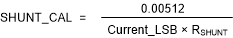
For the INA236 to report current values in Amperes, a constant conversion value must be written in the calibration register that is dependent on the selected CURRENT_LSB and the shunt resistance used in the application. The value of the calibration register is calculated based on Equation 1. The term CURRENT_LSB is the chosen LSB step size for the CURRENT register where the current is stored. Equation 2 shows the minimum value of CURRENT_LSB is based on the maximum expected current, and it directly defines the maximum resolution of the CURRENT register. While the smallest CURRENT_LSB value yields highest resolution, it is common to select a higher round-number (no higher than 8x) value for the CURRENT_LSB to simplify the conversion of the CURRENT.
The RSHUNT term is the resistance value of the external shunt used to develop the differential voltage across the IN+ and IN– pins. Use Equation 1 for ADCRANGE = 0. For ADCRANGE = 1, the value of SHUNT_CAL must be divided by 4.
where
- 0.00512 is an internal fixed value used to ensure scaling is maintained properly.
- CURRENT_LSB is a selected value for the current step size in amperes. Must be greater than or equal to CURRENT_LSB (minimum), but less than 8 x CURRENT_LSB(minimum) to reduce resolution loss.
- The value of SHUNT_CAL must be divided by 4 for ADCRANGE = 1.

Note that the current is calculated following a shunt voltage measurement based on the value set in the SHUNT_CAL register. If the value loaded into the SHUNT_CAL register is zero, the current value reported through the CURRENT register is also zero.
After programming the SHUNT_CAL register with the calculated value, the measured current in Amperes can be read from the CURRENT register. Use Equation 3 to calculate the final value scaled by the CURRENT_LSB:

where
- CURRENT is the value read from the CURRENT register
The power value can be read from the POWER register as a 16-bit value. Use Equation 4 to convert the power to Watts:

where
- POWER is the value read from the POWER register.
- CURRENT_LSB is selected value for the lsb size of the current calculation used in Equation 1.
Refer to Detailed Design Procedure for a design example using these equations.