SBOS956 December   2018 INA240-SEP

PRODUCTION DATA.  

  1. Features
  2. Applications
  3. Description
    1.     Device Images
      1.      Typical Application
      2.      Enhanced PWM Rejection
  4. Revision History
  5. Pin Configuration and Functions
    1.     Pin Functions
  6. Specifications
    1. 6.1 Absolute Maximum Ratings
    2. 6.2 ESD Ratings
    3. 6.3 Recommended Operating Conditions
    4. 6.4 Thermal Information
    5. 6.5 Electrical Characteristics
    6. 6.6 Typical Characteristics
  7. Detailed Description
    1. 7.1 Overview
    2. 7.2 Functional Block Diagram
    3. 7.3 Feature Description
      1. 7.3.1 Amplifier Input Signal
        1. 7.3.1.1 Enhanced PWM Rejection Operation
        2. 7.3.1.2 Input Signal Bandwidth
      2. 7.3.2 Selecting the Sense Resistor (RSENSE)
    4. 7.4 Device Functional Modes
      1. 7.4.1 Adjusting the Output Midpoint With the Reference Pins
      2. 7.4.2 Reference Pin Connections for Unidirectional Current Measurements
        1. 7.4.2.1 Ground Referenced Output
        2. 7.4.2.2 VS Referenced Output
      3. 7.4.3 Reference Pin Connections for Bidirectional Current Measurements
        1. 7.4.3.1 Output Set to External Reference Voltage
        2. 7.4.3.2 Output Set to Midsupply Voltage
        3. 7.4.3.3 Output Set to Mid-External Reference
        4. 7.4.3.4 Output Set Using Resistor Divider
      4. 7.4.4 Calculating Total Error
        1. 7.4.4.1 Error Sources
        2. 7.4.4.2 Reference Voltage Rejection Ratio Error
          1. 7.4.4.2.1 Total Error Example 1
          2. 7.4.4.2.2 Total Error Example 2
  8. Application and Implementation
    1. 8.1 Application Information
      1. 8.1.1 Input Filtering
    2. 8.2 Typical Applications
      1. 8.2.1 Inline Motor Current-Sense Application
        1. 8.2.1.1 Design Requirements
        2. 8.2.1.2 Detailed Design Procedure
        3. 8.2.1.3 Application Curve
      2. 8.2.2 Solenoid Drive Current-Sense Application
        1. 8.2.2.1 Design Requirements
        2. 8.2.2.2 Detailed Design Procedure
        3. 8.2.2.3 Application Curve
    3. 8.3 Do's and Don'ts
      1. 8.3.1 High-Precision Applications
      2. 8.3.2 Kelvin Connection from the Current-Sense Resistor
  9. Power Supply Recommendations
    1. 9.1 Power Supply Decoupling
  10. 10Layout
    1. 10.1 Layout Guidelines
      1. 10.1.1 Connection to the Current-Sense Resistor
    2. 10.2 Layout Example
  11. 11Device and Documentation Support
    1. 11.1 Receiving Notification of Documentation Updates
    2. 11.2 Community Resources
    3. 11.3 Trademarks
    4. 11.4 Electrostatic Discharge Caution
    5. 11.5 Glossary
  12. 12Mechanical, Packaging, and Orderable Information

Package Options

Mechanical Data (Package|Pins)
Thermal pad, mechanical data (Package|Pins)
Orderable Information

Adjusting the Output Midpoint With the Reference Pins

Figure 22 shows a test circuit for reference-divider accuracy. The INA240-SEP output is configurable to allow for unidirectional or bidirectional operation.
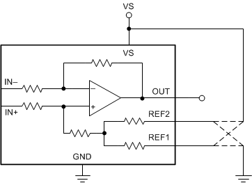
INA240-SEP ext_ref_test_divid_acc.gifFigure 22. Test Circuit For Reference Divider Accuracy

NOTE

Do not connect the REF1 pin or the REF2 pin to any voltage source lower than GND or higher than VS.

The output voltage is set by applying a voltage or voltages to the reference voltage inputs, REF1 and REF2. The reference inputs are connected to an internal gain network. There is no operational difference between the two reference pins.