SBOS662C July   2016  – December 2021 INA240

PRODUCTION DATA  

  1. Features
  2. Applications
  3. Description
  4. Revision History
  5. Device Comparison
  6. Pin Configuration and Functions
  7. Specifications
    1. 7.1 Absolute Maximum Ratings
    2. 7.2 ESD Ratings
    3. 7.3 Recommended Operating Conditions
    4. 7.4 Thermal Information
    5. 7.5 Electrical Characteristics
    6. 7.6 Typical Characteristics
  8. Detailed Description
    1. 8.1 Overview
    2. 8.2 Functional Block Diagram
    3. 8.3 Feature Description
      1. 8.3.1 Amplifier Input Signal
        1. 8.3.1.1 Enhanced PWM Rejection Operation
        2. 8.3.1.2 Input Signal Bandwidth
      2. 8.3.2 Selecting the Sense Resistor (RSENSE)
    4. 8.4 Device Functional Modes
      1. 8.4.1 Adjusting the Output Midpoint With the Reference Pins
      2. 8.4.2 Reference Pin Connections for Unidirectional Current Measurements
        1. 8.4.2.1 Ground Referenced Output
        2. 8.4.2.2 VS Referenced Output
      3. 8.4.3 Reference Pin Connections for Bidirectional Current Measurements
        1. 8.4.3.1 Output Set to External Reference Voltage
        2. 8.4.3.2 Output Set to Midsupply Voltage
        3. 8.4.3.3 Output Set to Mid-External Reference
        4. 8.4.3.4 Output Set Using Resistor Divider
      4. 8.4.4 Calculating Total Error
        1. 8.4.4.1 Error Sources
        2. 8.4.4.2 Reference Voltage Rejection Ratio Error
          1. 8.4.4.2.1 Total Error Example 1
          2. 8.4.4.2.2 Total Error Example 2
  9. Application and Implementation
    1. 9.1 Application Information
      1. 9.1.1 Input Filtering
    2. 9.2 Typical Applications
      1. 9.2.1 Inline Motor Current-Sense Application
        1. 9.2.1.1 Design Requirements
        2. 9.2.1.2 Detailed Design Procedure
        3. 9.2.1.3 Application Curve
      2. 9.2.2 Solenoid Drive Current-Sense Application
        1. 9.2.2.1 Design Requirements
        2. 9.2.2.2 Detailed Design Procedure
        3. 9.2.2.3 Application Curve
    3. 9.3 What to Do and What Not to Do
      1. 9.3.1 High-Precision Applications
      2. 9.3.2 Kelvin Connection from the Current-Sense Resistor
  10. 10Power Supply Recommendations
    1. 10.1 Power Supply Decoupling
  11. 11Layout
    1. 11.1 Layout Guidelines
      1. 11.1.1 Connection to the Current-Sense Resistor
    2. 11.2 Layout Example
  12. 12Device and Documentation Support
    1. 12.1 Documentation Support
      1. 12.1.1 Related Documentation
    2. 12.2 Receiving Notification of Documentation Updates
    3. 12.3 Support Resources
    4. 12.4 Trademarks
    5. 12.5 Electrostatic Discharge Caution
    6. 12.6 Glossary
  13. 13Mechanical, Packaging, and Orderable Information

Package Options

Mechanical Data (Package|Pins)
Thermal pad, mechanical data (Package|Pins)
Orderable Information

Typical Characteristics

at TA = 25°C, VS = 5 V, VCM = 12 V, and VREF = VS / 2 (unless otherwise noted)
GUID-8B07C1BD-7615-492E-B6B0-EBC4841BC30B-low.gif
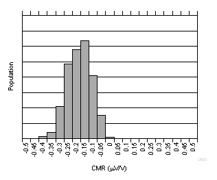
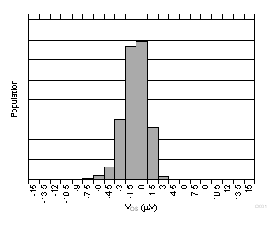
All gains
Figure 7-1 Input Offset Voltage Production Distribution
GUID-9ED8C419-E57D-41D9-B2C6-0A8232FF30F5-low.gif
All gains
Figure 7-3 Common-Mode Rejection Production Distribution
GUID-F8DD1151-563A-4E02-BB12-F54033FA55FD-low.gif
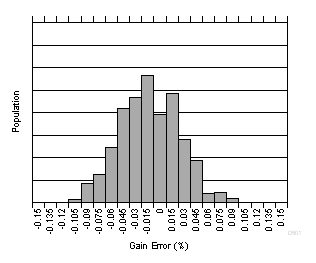
INA240A1
Figure 7-5 Gain Error Production Distribution
GUID-A97EC8F2-D704-4637-82C8-3BF2D5C06EDF-low.gif
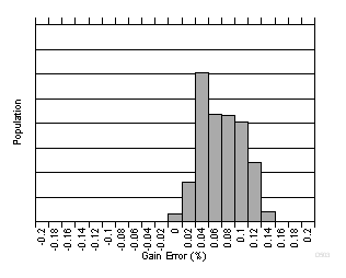
INA240A3
Figure 7-7 Gain Error Production Distribution
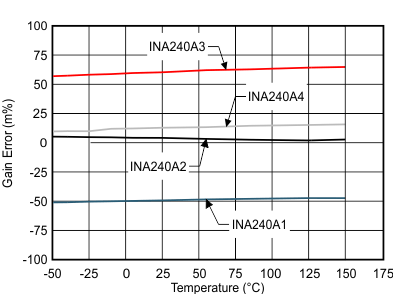
GUID-8B8B70BD-BB14-4C59-88ED-8274DA080CB1-low.gifFigure 7-9 Gain Error vs Temperature
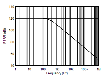
GUID-E0CD5DED-B807-428A-B78E-10856EEB1CD2-low.gifFigure 7-11 Power-Supply Rejection Ratio vs Frequency
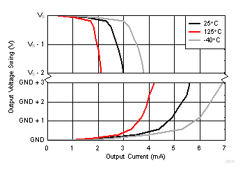
GUID-7AA6DA01-3CA7-4613-932D-ECE0F313D34F-low.gif
Figure 7-13 Output Voltage Swing vs Output Current
GUID-A6C43EEA-7222-45E3-A1BC-D6C13C07A432-low.gif
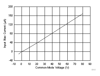
VS = 0 V
Figure 7-15 Input Bias Current vs Common-Mode Voltage
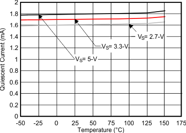
GUID-9B510D7F-229D-4E50-82F6-5AF02C53D3C1-low.gifFigure 7-17 Quiescent Current vs Temperature
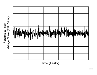
GUID-0BE9D1DE-5110-4AB3-9332-264616593E32-low.gif
VS = ±2.5 VVCM = 0 VVDIF = 0 V
VREF1 = VREF2 = 0 VInput referred
Figure 7-19 0.1-Hz to 10-Hz Voltage Noise
GUID-A0C04177-E557-4FD7-8A70-311D5F650864-low.gif
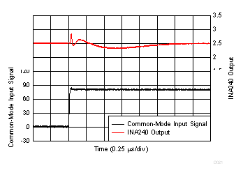
Rising edge
Figure 7-21 Common-Mode Voltage Transient Response
GUID-088C0B96-13F7-48CB-BC3B-F0B8FCAF5071-low.gif
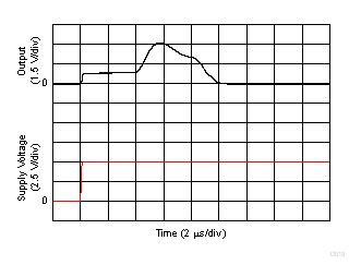
VREF1 = VREF2 = 0 V
Figure 7-23 Start-Up Response
GUID-CEC69EC6-8F36-43E0-B743-44FC8E72D3B2-low.gif
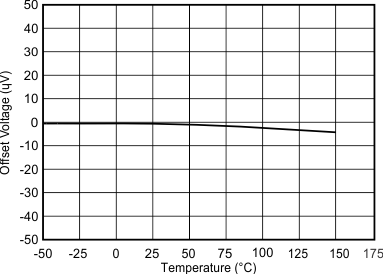
Figure 7-2 Offset Voltage vs Temperature
GUID-10CD667F-3C38-4D64-8EA3-83432CB53D3B-low.gif
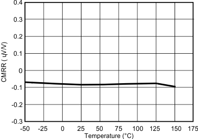
Figure 7-4 Common-Mode Rejection Ratio vs Temperature
GUID-9C7932E1-ED33-4343-8A62-B0AFB8EB30D0-low.gif
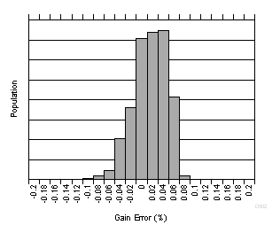
INA240A2
Figure 7-6 Gain Error Production Distribution
GUID-B35399FD-2193-4FEF-A2A6-C568B106737C-low.gif
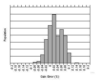
INA240A4
Figure 7-8 Gain Error Production Distribution
GUID-7FFCCA0B-3C9E-4541-BC78-73BD611C9D20-low.gif
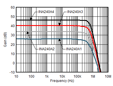
VCM = 0 VVDIF = 10-mVPP sine
Figure 7-10 Gain vs Frequency
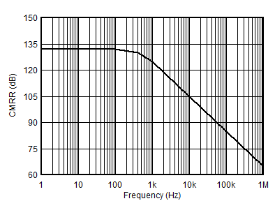
GUID-24E34F63-8ED5-4743-8504-727682DAC087-low.gifFigure 7-12 Common-Mode Rejection Ratio vs Frequency
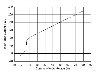
GUID-4E39D17B-8E8D-4D92-B3DF-0D825E63D73F-low.gif
VS = 5 V
Figure 7-14 Input Bias Current vs Common-Mode Voltage
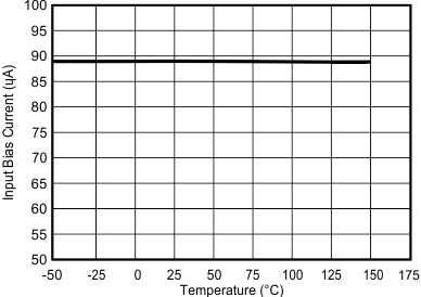
GUID-74B4F88B-41E7-44C9-AE0A-C6CF50AAC238-low.gif
Figure 7-16 Input Bias Current vs Temperature
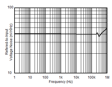
GUID-0688869A-6F60-4B7C-8E40-3221B2EE9D1B-low.gifFigure 7-18 Input-Referred Voltage Noise vs Frequency
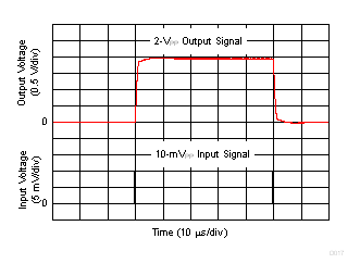
GUID-1D0FF0D6-F553-4F70-A2CE-5600FEC41BF8-low.gif
VREF1 = VREF2 = 0 V10-mVPP input step
Figure 7-20 Step Response
GUID-A518F84F-1970-48BF-87FC-9E961517553C-low.gif
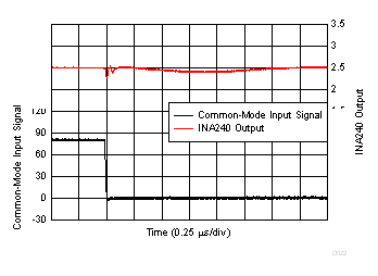
Falling edge
Figure 7-22 Common-Mode Voltage Transient Response