SBOS554C March 2012 – January 2021 INA282-Q1 , INA283-Q1 , INA284-Q1 , INA285-Q1 , INA286-Q1
PRODUCTION DATA
- 1 Features
- 2 Applications
- 3 Description
- 4 Revision History
- 5 Pin Configuration and Functions
- 6 Specifications
- 7 Detailed Description
- 8 Application and Implementation
- 9 Power Supply Recommendations
- 10Layout
- 11Device and Documentation Support
- 12Glossary
- 13Mechanical, Packaging, and Orderable Information
Package Options
Mechanical Data (Package|Pins)
Thermal pad, mechanical data (Package|Pins)
- DGK|8
Orderable Information
7.4.4.2 Example 2 INA286-Q1
Table 7-2 V+ = 5 V; VCM = 24 V; VREF1 = VREF2 = 0 V; VSENSE = 10 mV
| TERM | SYMBOL | EQUATION | TYPICAL VALUE | MAXIMUM VALUE |
|---|---|---|---|---|
| Initial input offset voltage | VOS | — | 20 μV | 70 μV |
| Added input offset voltage because of common-mode voltage | VOS_CM | 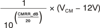 | 1.2 μV | 12 μV |
| Added input offset voltage because of reference voltage | VOS_REF |  | 34.8 μV | 92.2 μV |
| Total input offset voltage | VOS_Total | 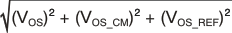 | 40.2 μV | 116.4 μV |
| Error from input offset voltage | Error_VOS | 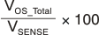 | 0.40% | 1.16% |
| Gain error | Error_Gain | — | 0.40% | 1.40% |
| Nonlinearity error | Error_Lin | — | 0.01% | 0.01% |
| Total error | — |

| 0.57% | 1.82% |