SBOS554C March   2012  – January 2021 INA282-Q1 , INA283-Q1 , INA284-Q1 , INA285-Q1 , INA286-Q1

PRODUCTION DATA  

  1. Features
  2. Applications
  3. Description
  4. Revision History
  5. Pin Configuration and Functions
  6. Specifications
    1. 6.1 Absolute Maximum Ratings
    2. 6.2 ESD Ratings
    3. 6.3 Recommended Operating Conditions
    4. 6.4 Thermal Information
    5. 6.5 Electrical Characteristics
    6. 6.6 Typical Characteristics
  7. Detailed Description
    1. 7.1 Overview
    2. 7.2 Functional Block Diagram
    3. 7.3 Feature Description
      1. 7.3.1 Selecting RS
      2. 7.3.2 Effective Bandwidth
      3. 7.3.3 Transient Protection
    4. 7.4 Device Functional Modes
      1. 7.4.1 Reference Pin Connection Options
        1. 7.4.1.1 Unidirectional Operation
          1. 7.4.1.1.1 Ground Referenced Output
          2. 7.4.1.1.2 V+ Referenced Output
        2. 7.4.1.2 Bidirectional Operation
          1. 7.4.1.2.1 External Reference Output
          2. 7.4.1.2.2 Splitting the Supply
          3. 7.4.1.2.3 Splitting an External Reference
      2. 7.4.2 Shutdown
      3. 7.4.3 Extended Negative Common-Mode Range
      4. 7.4.4 Calculating Total Error
        1. 7.4.4.1 Example 1 INA282-Q1
        2. 7.4.4.2 Example 2 INA286-Q1
  8. Application and Implementation
    1. 8.1 Application Information
      1. 8.1.1 Basic Connections
    2. 8.2 Typical Applications
      1. 8.2.1 Current Summing
        1. 8.2.1.1 Design Requirements
        2. 8.2.1.2 Detailed Design Procedures
        3. 8.2.1.3 Application Curve
      2. 8.2.2 Current Differencing
        1. 8.2.2.1 Design Requirements
        2. 8.2.2.2 Detailed Design Procedure
        3. 8.2.2.3 Application Curve
  9. Power Supply Recommendations
  10. 10Layout
    1. 10.1 Layout Guidelines
    2. 10.2 Layout Example
  11. 11Device and Documentation Support
    1. 11.1 Receiving Notification of Documentation Updates
    2. 11.2 Support Resources
    3. 11.3 Trademarks
    4. 11.4 Electrostatic Discharge Caution
  12. 12Glossary
  13. 13Mechanical, Packaging, and Orderable Information

Package Options

Mechanical Data (Package|Pins)
Thermal pad, mechanical data (Package|Pins)
Orderable Information
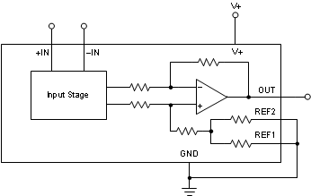
Ground Referenced Output

When using the INA28x-Q1 in this mode, both reference inputs are connected to ground; this configuration takes the output to the negative rail when there is 0V differential at the input (as Figure 7-2 shows).
GUID-BEBFE37D-F7AF-4051-A181-7C5A7F6765AE-low.gifFigure 7-2 Ground Referenced Output