SBOS995A October   2019  – November 2020 INA290-Q1

PRODUCTION DATA  

  1. Features
  2. Applications
  3. Description
  4. Revision History
  5. Pin Configuration and Functions
  6. Specifications
    1. 6.1 Absolute Maximum Ratings
    2. 6.2 ESD Ratings
    3. 6.3 Recommended Operating Conditions
    4. 6.4 Thermal Information
    5. 6.5 Electrical Characteristics
    6. 6.6 Typical Characteristics
  7. Detailed Description
    1. 7.1 Overview
    2. 7.2 Functional Block Diagram
    3. 7.3 Feature Description
      1. 7.3.1 Amplifier Input Common-Mode Range
        1. 7.3.1.1 Input-Signal Bandwidth
        2. 7.3.1.2 Low Input Bias Current
        3. 7.3.1.3 Low VSENSE Operation
        4. 7.3.1.4 Wide Fixed Gain Output
        5. 7.3.1.5 Wide Supply Range
    4. 7.4 Device Functional Modes
      1. 7.4.1 Unidirectional Operation
      2. 7.4.2 High Signal Throughput
  8. Application and Implementation
    1. 8.1 Application Information
      1. 8.1.1 RSENSE and Device Gain Selection
      2. 8.1.2 Input Filtering
    2. 8.2 Typical Application
      1. 8.2.1 Design Requirements
      2. 8.2.2 Detailed Design Procedure
        1. 8.2.2.1 Overload Recovery With Negative VSENSE
      3. 8.2.3 Application Curve
  9. Power Supply Recommendations
  10. 10Layout
    1. 10.1 Layout Guidelines
    2. 10.2 Layout Example
  11. 11Device and Documentation Support
    1. 11.1 Documentation Support
      1. 11.1.1 Related Documentation
    2. 11.2 Receiving Notification of Documentation Updates
    3. 11.3 Support Resources
    4. 11.4 Trademarks
    5. 11.5 Electrostatic Discharge Caution
    6. 11.6 Glossary
  12. 12Mechanical, Packaging, and Orderable Information

Package Options

Mechanical Data (Package|Pins)
Thermal pad, mechanical data (Package|Pins)
Orderable Information

Detailed Design Procedure

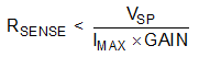
The maximum value of the current-sense resistor is calculated based choice of gain, value of the maximum current the be sensed (IMAX), and the power-supply voltage (VS). When operating at the maximum current, the output voltage must not exceed the positive output swing specification, VSP. Under the given design parameters, Equation 6 calculates the maximum value for RSENSE as 19.2 mΩ.

Equation 6. GUID-20200713-CA0I-RB5N-0HJ8-JNH9DN6GVL6K-low.gif

For this design example, a value of 15 mΩ is selected because, while the 15 mΩ is less than the maximum value calculated, 15 mΩ is still large enough to give adequate signal at the current-sense amplifier output.