SBOS995A October 2019 – November 2020 INA290-Q1
PRODUCTION DATA
- 1 Features
- 2 Applications
- 3 Description
- 4 Revision History
- 5 Pin Configuration and Functions
- 6 Specifications
- 7 Detailed Description
- 8 Application and Implementation
- 9 Power Supply Recommendations
- 10Layout
- 11Device and Documentation Support
- 12Mechanical, Packaging, and Orderable Information
Package Options
Mechanical Data (Package|Pins)
- DCK|5
Thermal pad, mechanical data (Package|Pins)
Orderable Information
8.1.2 Input Filtering
Input filters are not required for accurate measurements using the INA290-Q1, and use of filters in this location is not recommended. If filter components are used on the input of the amplifier, follow the guidelines in this section to minimize the effects on performance.
Based strictly on user design requirements, external filtering of the current signal may be desired. The initial location that can be considered for the filter is at the output of the current-sense amplifier. Although placing the filter at the output satisfies the filtering requirements, this location changes the low output impedance measured by any circuitry connected to the output voltage pin. The other location for filter placement is at the current-sense amplifier input pins. This location also satisfies the filtering requirement, but the components must be carefully selected to minimally impact device performance. Figure 8-1 shows a filter placed at the input pins.

Figure 8-1 Filter at Input Pins
External series resistance provides a source of additional measurement error, so keep the value of these series resistors to 10 Ω or less to reduce loss of accuracy. The internal bias network shown in Figure 8-1 creates a mismatch in input bias currents (see Figure 6-15, Figure 6-16, and Figure 6-17) when a differential voltage is applied between the input pins. If additional external series filter resistors are added to the circuit, a mismatch is created in the voltage drop across the filter resistors. This voltage is a differential error voltage in the shunt resistor voltage. In addition to the absolute resistor value, mismatch resulting from resistor tolerance can significantly impact the error because this value is calculated based on the actual measured resistance.
The measurement error expected from the additional external filter resistors can be calculated using Equation 4, where the gain error factor is calculated using Equation 5.

The gain error factor, shown in Equation 4, can be calculated to determine the gain error introduced by the additional external series resistance. Equation 4 calculates the deviation of the shunt voltage, resulting from the attenuation and imbalance created by the added external filter resistance. Table 8-2 provides the gain error factor and gain error for several resistor values.
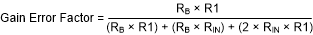
Where:
- RIN is the external filter resistance value.
- R1 is the INA290-Q1 input resistance value specified in Table 7-1.
- RB in the internal bias resistance, which is 6600 Ω ± 20%.
DEVICE (GAIN) | GAIN ERROR FACTOR | GAIN ERROR (%) |
|---|---|---|
A1 devices (20) | 0.99658 | –0.34185 |
A2 devices (50) | 0.99598 | –0.40141 |
A3 devices (100) | 0.99598 | –0.40141 |
A4 devices (200) | 0.99499 | –0.50051 |
A5 devices (500) | 0.99203 | –0.79663 |