SBOS977A March 2019 – May 2021 INA302-Q1 , INA303-Q1
PRODUCTION DATA
- 1 Features
- 2 Applications
- 3 Description
- 4 Revision History
- 5 Pin Configuration and Functions
- 6 Specifications
- 7 Detailed Description
- 8 Application and Implementation
- 9 Power Supply Recommendations
- 10Layout
- 11Device and Documentation Support
- 12Mechanical, Packaging, and Orderable Information
Package Options
Mechanical Data (Package|Pins)
- PW|14
Thermal pad, mechanical data (Package|Pins)
Orderable Information
7.3.3.2 Hysteresis
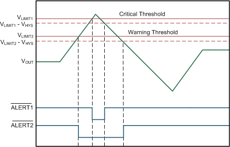
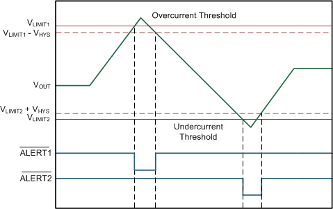
The hysteresis included in the comparators of the INA30x-Q1 reduces the possibility of oscillations in the alert outputs when the measured signal level is near the overlimit threshold level. For overrange events, the corresponding ALERTx pin is asserted when the output voltage (VOUT) exceeds the threshold set at either LIMITx pin. The output voltage must drop to less than the LIMITx pin threshold voltage by the hysteresis value in order for the ALERTx pin to deassert and return to the nominal high state. Likewise for underrange events, the corresponding ALERTx pin is also pulled low when the output voltage drops to less than the threshold set by either LIMITx pin. The ALERTx pin is released when the output voltage of the current-sense amplifier rises to greater than the set threshold plus hysteresis. Hysteresis functionality for both overrange and underrange events is shown in Figure 7-4 and Figure 7-5 for the INA302-Q1 and INA303-Q1, respectively.
 Figure 7-4 Comparator Hysteresis Behavior (INA302-Q1)
 Figure 7-5 Comparator Hysteresis Behavior (INA303-Q1)