SBOS977A March 2019 – May 2021 INA302-Q1 , INA303-Q1
PRODUCTION DATA
- 1 Features
- 2 Applications
- 3 Description
- 4 Revision History
- 5 Pin Configuration and Functions
- 6 Specifications
- 7 Detailed Description
- 8 Application and Implementation
- 9 Power Supply Recommendations
- 10Layout
- 11Device and Documentation Support
- 12Mechanical, Packaging, and Orderable Information
Package Options
Mechanical Data (Package|Pins)
- PW|14
Thermal pad, mechanical data (Package|Pins)
- PW|14
Orderable Information
7.3.3.1.1 Resistor-Controlled Current Limit
The typical approach to set the limit threshold voltage is to connect resistors from the two LIMITx pins to ground. The voltage developed across the RLIMIT1, RLIMIT2 resistors represents the desired fault current value at which the corresponding ALERTx pin becomes active. The values for the RLIMIT1, RLIMIT2 resistors are calculated using Equation 3:
Equation 3. 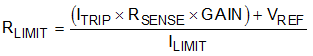
where
- ITRIP is the desired out-of-range current threshold.
- RSENSE is the current-sensing resistor.
- GAIN is the gain option of the device selected.
- VREF is the voltage applied to the REF pin.
- ILIMIT is the limit threshold output current for the selected comparator, typically 80 µA.
Note:
When solving for the value of RLIMIT, the voltage at the corresponding LIMITx pin as determined by the product of RLIMIT and ILIMIT must not exceed the compliance voltage of VS – 0.6 V.