SBOS562G August 2011 – June 2020 INA826
PRODUCTION DATA.
- 1 Features
- 2 Applications
- 3 Description
- 4 Revision History
- 5 Device Comparison Table
- 6 Pin Configuration and Functions
- 7 Specifications
-
8 Detailed Description
- 8.1 Overview
- 8.2 Functional Block Diagram
- 8.3 Feature Description
- 8.4 Device Functional Modes
- 9 Application and Implementation
- 10Power Supply Recommendations
- 11Layout
- 12Device and Documentation Support
- 13Mechanical, Packaging, and Orderable Information
Package Options
Mechanical Data (Package|Pins)
Thermal pad, mechanical data (Package|Pins)
Orderable Information
8.3.1 Inside the INA826
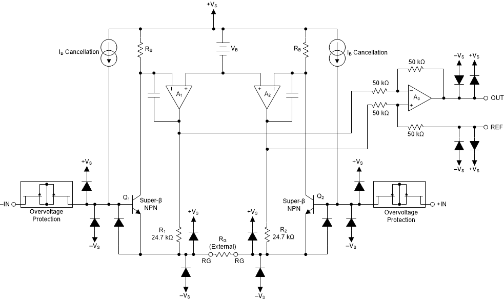
See the Functional Block Diagram section for a simplified representation of the INA826. A more detailed diagram, shown in Figure 58, provides additional insight into the INA826 operation.
Each input is protected by two field-effect transistors (FETs) that provide a low series resistance under normal signal conditions, and preserve excellent noise performance. When excessive voltage is applied, these transistors limit input current to approximately 8 mA.
The differential input voltage is buffered by Q1 and Q2 and is impressed across RG, causing a signal current to flow through RG, R1, and R2. The output difference amplifier, A3, removes the common-mode component of the input signal and refers the output signal to the REF terminal.
The equations shown in Figure 58 describe the output voltages of A1 and A2. The VBE and voltage drop across R1 and R2 produce output voltages on A1 and A2 that are approximately 0.8 V higher than the input voltages.
