SBOS938C October   2018  – June 2020 INA901-SP

PRODUCTION DATA.  

  1. Features
  2. Applications
  3. Description
    1.     Simplified Schematic
  4. Revision History
  5. Pin Configuration and Functions
    1.     Pin Functions
  6. Specifications
    1. 6.1 Absolute Maximum Ratings
    2. 6.2 ESD Ratings
    3. 6.3 Recommended Operating Conditions
    4. 6.4 Thermal Information
    5. 6.5 Electrical Characteristics
    6. 6.6 Quality Conformance Inspection
    7. 6.7 Typical Characteristics
  7. Detailed Description
    1. 7.1 Overview
    2. 7.2 Functional Block Diagram
    3. 7.3 Feature Description
      1. 7.3.1 Basic Connection
      2. 7.3.2 Selecting RS
      3. 7.3.3 Transient Protection
    4. 7.4 Device Functional Modes
      1. 7.4.1 First- or Second-Order Filtering
      2. 7.4.2 Accuracy Variations as a Result of VSENSE and Common-Mode Voltage
        1. 7.4.2.1 Normal Case 1: VSENSE ≥ 20 mV, VCM ≥ VS
        2. 7.4.2.2 Normal Case 2: VSENSE ≥ 20 mV, VCM < VS
        3. 7.4.2.3 Low VSENSE Case 1: VSENSE < 20 mV, –15 V ≤ VCM < 0; and Low VSENSE Case 3: VSENSE < 20 mV, VS < VCM ≤ 65 V
        4. 7.4.2.4 Low VSENSE Case 2: VSENSE < 20 mV, 0 V ≤ VCM ≤ VS
  8. Application and Implementation
    1. 8.1 Application Information
    2. 8.2 Typical Application
      1. 8.2.1 Design Requirements
      2. 8.2.2 Detailed Design Procedure
      3. 8.2.3 Application Curves
  9. Power Supply Recommendations
  10. 10Layout
    1. 10.1 Layout Guidelines
      1. 10.1.1 RFI and EMI
    2. 10.2 Layout Example
  11. 11Device and Documentation Support
    1. 11.1 Documentation Support
      1. 11.1.1 Related Documentation
    2. 11.2 Receiving Notification of Documentation Updates
    3. 11.3 Community Resources
    4. 11.4 Trademarks
    5. 11.5 Electrostatic Discharge Caution
    6. 11.6 Glossary
  12. 12Mechanical, Packaging, and Orderable Information

Package Options

Mechanical Data (Package|Pins)
Thermal pad, mechanical data (Package|Pins)
Orderable Information

Low VSENSE Case 2: VSENSE < 20 mV, 0 V ≤ VCM ≤ VS

This region of operation is the least accurate for the INA901-SP. To achieve the wide input common-mode voltage range, this device uses two op amp front ends in parallel. One op amp front end operates in the positive input common-mode voltage range, and the other in the negative input region. For this case, neither of these two internal amplifiers dominates and overall loop gain is very low. Within this region, VOUT approaches voltages close to linear operation levels for Normal Case 2.

This deviation from linear operation becomes greatest the closer VSENSE approaches 0 V. Within this region, when VSENSE approaches 20 mV, device operation is closer to that described by Normal Case 2. Figure 18 shows this behavior for the INA901-SP. The VOUT maximum peak for this case is determined by maintaining a constant VS, setting VSENSE = 0 mV, and sweeping VCM from 0 V to VS. The exact VCM at which VOUT peaks during this case varies from device to device. The maximum peak voltage for the INA901-SP is 0.4 V.
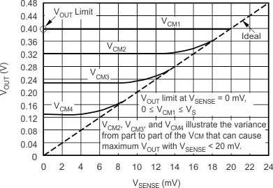
INA901-SP ai_exam_case2_sbos938.gif
Figure 18. Example for Low VSENSE Case 2 (INA901-SP, Gain = 20)