SLLSEY7F June 2017 – April 2020 ISO1211 , ISO1212
PRODUCTION DATA.
- 1 Features
- 2 Applications
- 3 Description
- 4 Revision History
- 5 Pin Configuration and Functions
-
6 Specifications
- 6.1 Absolute Maximum Ratings
- 6.2 ESD Ratings
- 6.3 Recommended Operating Conditions
- 6.4 Thermal Information
- 6.5 Power Ratings
- 6.6 Insulation Specifications
- 6.7 Safety-Related Certifications
- 6.8 Safety Limiting Values
- 6.9 Electrical Characteristics—DC Specification
- 6.10 Switching Characteristics—AC Specification
- 6.11 Insulation Characteristics Curves
- 6.12 Typical Characteristics
- 7 Parameter Measurement Information
- 8 Detailed Description
- 9 Application and Implementation
- 10Power Supply Recommendations
- 11Layout
- 12Device and Documentation Support
- 13Mechanical, Packaging, and Orderable Information
Package Options
Refer to the PDF data sheet for device specific package drawings
Mechanical Data (Package|Pins)
- D|8
Thermal pad, mechanical data (Package|Pins)
Orderable Information
9.2.1.2.7 Status LEDs
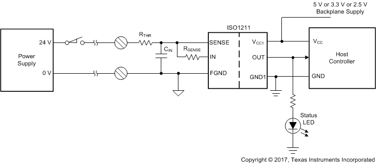
The outputs of the ISO121x devices can be used to drive status LEDs on the controller side as shown in Figure 26. The output buffers of the ISO121x can provide 4-mA, 3-mA, and 2-mA currents while working at VCC1 values of 5 V, 3.3 V, and 2.5 V respectively.
In some cases, placing the LED on the field side is desirable although it is powered from VCC1. In such cases, the signal carrying current to the LED can be routed in an inner layer without compromising the isolation of the digital-input module. For more information, see the Layout Guidelines section.
 Figure 26. Using ISO121x Outputs to Drive Status LEDs