SLLSEB6F July 2012 – December 2022 ISO1540 , ISO1541
PRODUCTION DATA
- 1 Features
- 2 Applications
- 3 Description
- 4 Revision History
- 5 Pin Configuration and Functions
-
6 Specifications
- 6.1 Absolute Maximum Ratings
- 6.2 ESD Ratings
- 6.3 Recommended Operating Conditions
- 6.4 Thermal Information
- 6.5 Power Ratings
- 6.6 Insulation Specifications
- 6.7 Safety-Related Certifications
- 6.8 Safety Limiting Values
- 6.9 Electrical Characteristics
- 6.10 Supply Current Characteristics
- 6.11 Timing Requirements
- 6.12 Switching Characteristics
- 6.13 Insulation Characteristics Curves
- 6.14 Typical Characteristics
- 7 Detailed Description
- 8 Application and Implementation
- 9 Power Supply Recommendations
- 10Layout
- 11Device and Documentation Support
- 12Mechanical, Packaging, and Orderable Information
Package Options
Mechanical Data (Package|Pins)
- D|8
Thermal pad, mechanical data (Package|Pins)
Orderable Information
8.2.2 Detailed Design Procedure
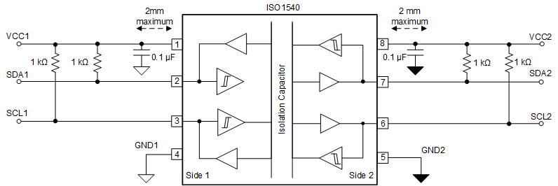
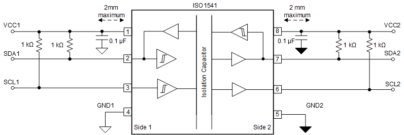
The power-supply capacitor with a value of 0.1-µF must be placed as close to the power supply pins as possible. The recommended placement of the capacitors must be 2-mm maximum from input and output power supply pins (VCC1 and VCC2).
The maximum load permissible on the input lines, SDA1 and SCL1, is ≤ 40 pF and on the output lines, SDA2 and SCL2, is ≤ 400 pF.
The minimum pullup resistors on the input lines, SDA1 and SCL1 to VCC1 must be selected in such a way that input current drawn is ≤ 3.5 mA. The minimum pullup resistors on the input lines, SDA2 and SCL2, to VCC2 must be selected in such a way that output current drawn is ≤ 35 mA. The maximum pullup resistors on the input lines (SDA1 and SCL1) to VCC1 and on output lines (SDA1 and SCL1) to VCC2, depends on the load and rise time requirements on the respective lines.
 Figure 8-5 Typical ISO1540 Circuit Hookup
 Figure 8-6 Typical ISO1541 Circuit Hookup