SLASEY9B December 2019 – February 2023 ISO6731
PRODUCTION DATA
- 1 Features
- 2 Applications
- 3 Description
- 4 Revision History
- 5 Pin Configuration and Functions
-
6 Specifications
- 6.1 Absolute Maximum Ratings
- 6.2 ESD Ratings
- 6.3 Recommended Operating Conditions
- 6.4 Thermal Information
- 6.5 Power Ratings
- 6.6 Insulation Specifications
- 6.7 Safety-Related Certifications
- 6.8 Safety Limiting Values
- 6.9 Electrical Characteristics—5-V Supply
- 6.10 Supply Current Characteristics—5-V Supply
- 6.11 Electrical Characteristics—3.3-V Supply
- 6.12 Supply Current Characteristics—3.3-V Supply
- 6.13 Electrical Characteristics—2.5-V Supply
- 6.14 Supply Current Characteristics—2.5-V Supply
- Electrical Characteristics—1.8-V Supply
- 6.15 Supply Current Characteristics—1.8-V Supply
- 6.16 Switching Characteristics—5-V Supply
- 6.17 Switching Characteristics—3.3-V Supply
- 6.18 Switching Characteristics—2.5-V Supply
- 6.19 Switching Characteristics—1.8-V Supply
- 6.20 Insulation Characteristics Curves
- 6.21 Typical Characteristics
- 7 Parameter Measurement Information
- 8 Detailed Description
- 9 Application and Implementation
- 10Power Supply Recommendations
- 11Layout
- 12Device and Documentation Support
- 13Mechanical, Packaging, and Orderable Information
Package Options
Mechanical Data (Package|Pins)
- DW|16
Thermal pad, mechanical data (Package|Pins)
- DW|16
Orderable Information
3 Description
The ISO6731 device is a high-performance, triple-channel digital isolators ideal for cost-sensitive applications requiring up to 5000 VRMS isolation ratings per UL 1577. This device is also certified by VDE, TUV, CSA, and CQC.
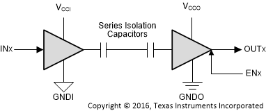
The ISO6731 devics provides high electromagnetic immunity and low emissions at low power consumption, while isolating CMOS or LVCMOS digital I/Os. Each isolation channel has a logic input and output buffer separated by TI's double capacitive silicon dioxide (SiO2) insulation barrier. This device comes with enable pins which can be used to put the respective outputs in high impedance for multi-master driving applications. The ISO6731 device has two forward and one reverse-direction channels. In the event of input power or signal loss, the default output is high for the device without suffix F and low for the device with suffix F. See Device Functional Modes section for further details.
Used in conjunction with isolated power supplies, this device helps prevent noise currents on data buses, such as UART, SPI, RS-485, RS-232, and CAN from damaging sensitive circuitry. Through innovative chip design and layout techniques, the electromagnetic compatibility of the ISO6731 device has been significantly enhanced to ease system-level ESD, EFT, surge, and emissions compliance. The ISO6731 device is available in a 16-pin SOIC wide-body (DW) package and is a pin-to-pin upgrade to the older generations.
| PART NUMBER (1) | PACKAGE | BODY SIZE (NOM) |
|---|---|---|
| ISO6731, ISO6731F | SOIC (DW) | 10.30 mm × 7.50 mm |
