SLLSF54D October 2017 – March 2020 ISO7041
PRODUCTION DATA.
- 1 Features
- 2 Applications
- 3 Description
- 4 Revision History
- 5 Device Comparison Table
- 6 Pin Configuration and Functions
-
7 Specifications
- 7.1 Absolute Maximum Ratings
- 7.2 ESD Ratings
- 7.3 Recommended Operating Conditions
- 7.4 Thermal Information
- 7.5 Power Ratings
- 7.6 Insulation Specifications
- 7.7 Safety-Related Certifications
- 7.8 Safety Limiting Values
- 7.9 Electrical Characteristics 5V Supply
- 7.10 Supply Current Characteristics 5V Supply
- 7.11 Electrical Characteristics 3.3V Supply
- 7.12 Supply Current Characteristics 3.3V Supply
- 7.13 Electrical Characteristics 2.5V Supply
- 7.14 Supply Current Characteristics 2.5V Supply
- 7.15 Electrical Characteristics 1.8V Supply
- 7.16 Supply Current Characteristics 1.8V Supply
- 7.17 Switching Characteristics
- 7.18 Insulation Characteristics Curves
- 7.19 Typical Characteristics
- 8 Parameter Measurement Information
- 9 Detailed Description
- 10Application and Implementation
- 11Power Supply Recommendations
- 12Layout
- 13Device and Documentation Support
- 14Mechanical, Packaging, and Orderable Information
Package Options
Mechanical Data (Package|Pins)
- DBQ|16
Thermal pad, mechanical data (Package|Pins)
Orderable Information
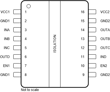
6 Pin Configuration and Functions
ISO7041 DBQ Package
16-Pin QSOP
Top View

Pin Functions
| PIN | I/O | DESCRIPTION | |
|---|---|---|---|
| NAME | NO. | ||
| EN1 | 7 | I | Refresh enable 1. Refresh is enabled when the EN1 pin is connected to GND1. Disable refresh by connecting the EN1 pin high to VCC1. EN1 and EN2 must be connected to the same logic state to enable or disable refresh. |
| EN2 | 10 | I | Refresh enable 2. Refresh is enabled when the EN2 pin is connected to GND2. Disable refresh by connecting the EN2 pin high to VCC2. EN1 and EN2 must be connected to the same logic state to enable or disable refresh. |
| GND1 | 2 | — | Ground connection for VCC1 |
| 8 | |||
| GND2 | 9 | — | Ground connection for VCC2 |
| 15 | |||
| INA | 3 | I | Input, channel A |
| INB | 4 | I | Input, channel B |
| INC | 5 | I | Input, channel C |
| IND | 11 | I | Input, channel D |
| OUTA | 14 | O | Output, channel A |
| OUTB | 13 | O | Output, channel B |
| OUTC | 12 | O | Output, channel C |
| OUTD | 6 | O | Output, channel D |
| VCC1 | 1 | — | Power supply, side 1 |
| VCC2 | 16 | — | Power supply, side 2 |